LC520 Overclock

kefkafloyd

New Tinkerer
May 22, 2023
20
20
3
Massachusetts
www.userlandia.com
Really cool article, thanks for sharing! I definitely can see documentation error leading folks to think the LC 550 and CC II logic boards were substantially different when they actually aren't. I do wonder what controls the different gestalt IDs though?

Macintosh LC 520 = 56
Macintosh LC 550 = 80
Macintosh Color Classic II = 83

The resistors affecting CPU speed would explain 520/550, but LC 550/CC II? Something from the chassis? Video resolution from the sense code?

I believe on these machines the Gestalt is determined from some combination of CPU speed and sense pin detection on the machine's logic board connector. The ROMs are identical between LC 520, LC 550, and Color Classic II and they all use the same System Enabler 403. My LC 550 board inside the Color Classic simply comes up as "Macintosh", but it does show the Color Classic icon. Put the same board in my Mac TV and it shows up as "Macintosh" but with a Hook chassis icon instead.

You'll note in JDW's 67Hz 640x480 mod video that his LC 520 board does identify as an LC 520 inside of the modified Color Classic. But I don't know if he tried that in his machine before the modifications.

Looking at the System Enabler 403 STR# resource the strings for IDs 80 and 83 (LC 550 and CC II) are blank. Of these three machines only the LC 520 has a proper string value at its gestalt. All three of these machines need Enabler 403 to boot, though. A reasonable guess is that the enabler was never updated when the 550/CC II were speed bumped. If I were to edit the names into strings 80 and 83 in it I bet they'd show up correctly.

Apple is not above using jumpers, resistors, or bridges along with the CPU speed to set gestalts—the difference between an LC 475 and Q605 is Jumper J18. Changing chip speeds on other boards will make different gestalts come up as well. http://www.rgaros.nl/gestalt/chapters/ch-19.html

Back to the original question from that article my LC 550 board is Rev B (4.5 Volt PRAM battery) so if you confirmed Rev A (3.6 Volt PRAM battery) then neither have R80 populated.
Excellent, thanks for confirming this!
 
  • Love
  • Like
Reactions: Fizzbinn and JDW

Fizzbinn

Tinkerer
Nov 29, 2021
241
244
43
Charlottesville, VA
Back to the original question, from that article my LC 550 board is Rev B (4.5 Volt PRAM battery) so if you confirmed Rev A (3.6 Volt PRAM battery) then neither have R80 populated.

@Fizzbinn you’re amazing!
And @kefkafloyd , thank you too!

I just posted the question about the 550 Rev. B board on FaceBook, so let’s see if that brings forth the final answer more quickly…

View attachment 23762

I think there was some confusion, my LC 550 board is a Rev. B (820-0595-A, 4.5V PRAM battery with velcro) and @kefkafloyd 's LC 550 board is a Rev. A (820-0368-A, 3.6V 1/2 AA PRAM battery) so we have confirmed both lack all 4 resistors, although more confirmation is never a bad idea!

Summarizing my newfound understanding:

SpeedLogic Board silk screenRC67, R75, R79, R80 InstalledPRAM Battery Type
LC 52025 MHz820-0368-A, 1993Yes3.6V 1/2 AA
LC 550 (Rev. A Logic Board)33 MHz820-0368-A, 1993No3.6V 1/2 AA
LC 550 (Rev. B Logic Board)33 MHz820-0595-A, 1993,94No4.5V Alkaline
Color Classic II33 MHz820-0368-A, 1993No3.6V 1/2 AA
 
Last edited:
  • Love
Reactions: JDW

kefkafloyd

New Tinkerer
May 22, 2023
20
20
3
Massachusetts
www.userlandia.com
Of note, there's another way to identify boards: their serial schemas.

I've noticed two different schemas for 520s: EZxxxxxxDY7 and DWxxxxxxDY7. The DW boards are the later ones (the serial labels say Rev D). I think the difference is that the EZ boards were made in Singapore while the DW ones were made in Malaysia. At least, that's what I've noticed.

Interestingly, both LC 550 revisions have the same schema of DWxxxxxx1X9. All the CC II and 550 boards I've seen have followed it. The newer revision will have "CUDA" on the serial label.

There's also LC 550 boards which were originally meant for half-AAs that have factory bodges to use the alkaline battery. They still have 820-0368-A on their silkscreen, so they're not the later revision boards.
 
  • Like
Reactions: JDW

JDW

Administrator
Staff member
Founder
Sep 2, 2021
2,326
1,885
113
54
Japan
youtube.com
You'll note in JDW's 67Hz 640x480 mod video that his LC 520 board does identify as an LC 520 inside of the modified Color Classic. But I don't know if he tried that in his machine before the modifications.
I did indeed test my LC520 motherboard in my Color Classic with the standard 60Hz 68.4V "VGA mod" (640x480 resolution) installed. But as you may know, the 520 and 550 and stock CC boards are NOT compatible with the standard VGA mod, and that's why I more recently released a video about my switch to the 67Hz 84V 13" High Resolution Mod, which allows use of ALL COMPATIBLE motherboards, including the LC575.

When using the stock CC motherboard in the CC with the 68.4V VGA Mod, you get a black screen, but the machine still boots.

When you using the LC520 motherboard in the CC with 68.4V VGA Mod, you get a display on the CRT, but the vertical sync is lost and it endlessly rolls vertically like this:


I've never tested the LC520 board in my CC in its stock condition (i.e., at 512x384 resolution).


I think there was some confusion, my LC 550 board is a Rev. B (820-0595-A, 4.5V PRAM battery with velcro)...

🤦‍♂️ Yes, my eyes sadly and shockingly overlooked that when I first spotted your photos, and subsequent to that I read @kefkafloyd 's reply saying, "No idea if R80 is populated on a Rev B board." And for some reason my silly brain fixated on that statement and neglected to ponder your crystal clear photos!

Ack! I must be experiencing a Brain Cloud.
BrainCloud.png


@Fizzbinn
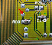
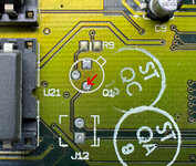
I overlaid your LC550 Rev. B board's TOP & BTM photos, distorted them slightly so all pads would align, then I flipped the PCB TOP horizontally so it would be super easy to flip back and forth and see where R80 pads lead. Sadly, one teensy tight thru-hole pad (see rightmost arrow below) seems to connect to inner traces, and the other pad (shown by the arrow at left below) leads us elsewhere on the board.

1760409743598.png


1760409726136.png


So I still have no idea what resistor R80 is supposed to do, and without a schematic its much more troublesome to find out.

What seems rather clear though is that we should remove 4 resistors, not simply 3.

@Drake hasn't been replying back in this thread, and Uniserver stopped all online replies years ago and is now unreachable, so it's not clear if either of them experienced issues after their 3-resistor Overclock. I've also not been able to Google-up anyone else whose followed their lead in removing only 3 resistors either.
 

Fizzbinn

Tinkerer
Nov 29, 2021
241
244
43
Charlottesville, VA
I overlaid your LC550 Rev. B board's TOP & BTM photos, distorted them slightly so all pads would align, then I flipped the PCB TOP horizontally so it would be super easy to flip back and forth and see where R80 pads lead. Sadly, one teensy tight thru-hole pad (see rightmost arrow below) seems to connect to inner traces, and the other pad (shown by the arrow at left below) leads us elsewhere on the board.

1760409743598.png


1760409726136.png


So I still have no idea what resistor R80 is supposed to do, and without a schematic its much more troublesome to find out.

What seems rather clear though is that we should remove 4 resistors, not simply 3.

Hmm, from your sleuthing perhaps the reason why others left off R80 as needing to be removed is that is was vestigial? The Q1 component is missing from both the LC 520 and LC 550. Its possible inter-layer connections connect R80 in a meaningful way to other components but maybe not, it seems within reason that it could be tied up in whatever lead Apple to build but not populate Q1 and J12... Like documentation errors it seems somewhat likely that when Q1 and J12 where deemed not needed the supporting R80 was forgotten to be removed and this was fixed in subsequent versions. Just a guess. If I was trying to convert a 520 board to a 550 board I'd remove it nonetheless.
 
Last edited:
  • Like
Reactions: JDW

kefkafloyd

New Tinkerer
May 22, 2023
20
20
3
Massachusetts
www.userlandia.com
I did indeed test my LC520 motherboard in my Color Classic with the standard 60Hz 68.4V "VGA mod" (640x480 resolution) installed. But as you may know, the 520 and 550 and stock CC boards are NOT compatible with the standard VGA mod, and that's why I more recently released a video about my switch to the 67Hz 84V 13" High Resolution Mod, which allows use of ALL COMPATIBLE motherboards, including the LC575.

When using the stock CC motherboard in the CC with the 68.4V VGA Mod, you get a black screen, but the machine still boots.

When you using the LC520 motherboard in the CC with 68.4V VGA Mod, you get a display on the CRT, but the vertical sync is lost and it endlessly rolls vertically like this:


I've never tested the LC520 board in my CC in its stock condition (i.e., at 512x384 resolution).
Thanks for the info. I could not recall what your tests with previous mods were, so this is helpful information.

The stock CC board not working at 640x480 60Hz makes sense, because I could find no evidence of the LC II architecture supporting 60Hz 640x480 output. It wouldn't recognize that combination of sense pins, ergo no video. It does support 640x480 at 67Hz (as you've proven) as documented. I've run it at 640x480 67Hz in my Mac TV with no issues.

The LC 520 board should absolutely work at stock resolution (512x384) inside a CC, since my LC 550 board does. I'm sure I've read people using that configuration with no issues.

The LC III architecture (of which the 520/550 is based) does officially support 640x480 at 60Hz VGA output according to its tech note. It's possible that a 60Hz VGA mod for a 520/550 board may be different than one for the Mystic, but comparing the 640x480 60Hz timings from the LC 475 and LC III technotes they appear identical. I'm not sure why it would lose vertical sync in that scenario unless there's undocumented differences in the video modes.
 

kefkafloyd

New Tinkerer
May 22, 2023
20
20
3
Massachusetts
www.userlandia.com
Hmm, from your sleuthing perhaps the reason why others left off R80 as needing to be removed is that is was vestigial? The Q1 component is missing from both the LC 520 and LC 550. Its possible inter-layer connections connect R80 in a meaningful way to other components but maybe not, it seems within reason that it could be tied up in whatever lead Apple to build but not populate Q1 and J12... Like documentation errors it seems somewhat likely that when Q1 and J12 where deemed not needed the supporting R80 was forgotten to be removed and this was fixed in subsequent versions. Just a guess. If I was trying to convert a 520 board to a 550 board I'd remove it nonetheless.
I am curious what a transistor and a jumper in line would be used for. I'm no board expert but vestigial R80 seems right.
 
  • Like
Reactions: Fizzbinn

JDW

Administrator
Staff member
Founder
Sep 2, 2021
2,326
1,885
113
54
Japan
youtube.com
I've run [the stock CC board] at 640x480 67Hz in my Mac TV with no issues.

As shown in my VGA mod conversion video, while the stock CC board does work with the 67Hz 84V 640x480 mod, the black borders at left and right of the CRT display area are thicker than when using an LC 575 or LC 520 board. And while it’s not technically a massive difference, it is noticeable.

This is rather mysterious because I would expect all compatible motherboards to display on the CRT in the same way.
 

kefkafloyd

New Tinkerer
May 22, 2023
20
20
3
Massachusetts
www.userlandia.com
As shown in my VGA mod conversion video, while the stock CC board does work with the 67Hz 84V 640x480 mod, the black borders at left and right of the CRT display area are thicker than when using an LC 575 or LC 520 board. And while it’s not technically a massive difference, it is noticeable.

This is rather mysterious because I would expect all compatible motherboards to display on the CRT in the same way.
Have you forgotten my post from a while back about why those borders differ? ;)
 
  • Love
Reactions: JDW

JDW

Administrator
Staff member
Founder
Sep 2, 2021
2,326
1,885
113
54
Japan
youtube.com
Yes, I actually did forget about that your excellent post. And that is due to me being very forgetful about pretty much everything. Sorry. It’s that bad memory that led me to get into YouTube in the first place because I originally made the videos for myself so I could remember what I’ve done in the past! Thank you for linking it for me as a reminder!

But basically my previous post was simply trying to say that even though you said “no issues,“ I did want to point out one minor issue about the display area with when using the stock CC board in a CC with the 67Hz 84V mod. That’s all.
 

kefkafloyd

New Tinkerer
May 22, 2023
20
20
3
Massachusetts
www.userlandia.com
But basically my previous post was simply trying to say that even though you said “no issues,“ I did want to point out one minor issue about the display area with when using the stock CC board in a CC with the 67Hz 84V mod. That’s all.
That is true. I'd call it a difference, because it doesn't bother me that much, but it could definitely be an issue for others.
 

JDW

Administrator
Staff member
Founder
Sep 2, 2021
2,326
1,885
113
54
Japan
youtube.com
...vestigial R80 seems right.
I cannot visually trace the side of R80 which leads to a tiny round thru-hole, but I can visually trace the other side of R80 which leads to this large round pad with solder on it...

R80_RoundPadSide_LC520.jpg

The same pad on the flipside of my LC520 motherboard...

R80_RoundPadSide_ComponentSide_LC520.jpg

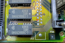
I re-checked visually 3 times and found it leads to the round pad just above the square pad on the non-existing ROM socket pads shown here...

R80_ROMsocket-RoundPad_LC520.jpg

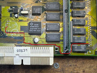
Here's a zoomed-out view showing start to finish on the component side of the LC520 motherboard...

R80_RoundPadSide_ToROMSocket_LC520.jpg

But here the strange part. When I set my multimeter to Continuity check mode and put one probe at one end and the other probe at the other, I get no beep. And when I switch my meter to measure Ohms, I read about 17MΩ. This doesn't make a lot of sense, but I tried measuring multiple times and that is what I get (roughly) each time.

Since the LC520 and 550 boards seem to be quite nearly the same, this info would apply to the 550 board as well.
 
  • Like
Reactions: Fizzbinn

dougg3

Tinkerer
Jan 10, 2022
28
43
13
www.downtowndougbrown.com
I re-checked visually 3 times and found it leads to the round pad just above the square pad on the non-existing ROM socket pads shown here...

That pin (pin 2) on the ROM SIMM socket is VPP, which is 12V power for allowing EEPROM chips of the era to be reprogrammed in-system. Pin 2 was also the A0 address line on older Macs, but Apple began using it for VPP in the Quadra era, presumably after realizing that A0 and A1 didn't need to be routed to the socket.

I haven't looked in depth at my 550 board, but it's likely to be similar to the circuit in Apple's leaked Color Classic schematics on page 3. I believe the transistor's purpose is to allow you to enable or disable VPP programmatically. There are some useful notes on the Color Classic schematics about it.

The Color Classic board actually has two transistors, so I wouldn't be surprised if there's another unpopulated transistor nearby on the 520/550 board too.

Edit: I think I spoke too soon; after looking closer at your pictures, it's actually pin 3. That's /WE which is write enable, also involved in in-system programming of ROM SIMMs. Maybe not exactly the same as the Color Classic schematic, but it might have some clues.
 
  • Like
Reactions: Fizzbinn and JDW

kefkafloyd

New Tinkerer
May 22, 2023
20
20
3
Massachusetts
www.userlandia.com
That pin (pin 2) on the ROM SIMM socket is VPP, which is 12V power for allowing EEPROM chips of the era to be reprogrammed in-system. Pin 2 was also the A0 address line on older Macs, but Apple began using it for VPP in the Quadra era, presumably after realizing that A0 and A1 didn't need to be routed to the socket.

I haven't looked in depth at my 550 board, but it's likely to be similar to the circuit in Apple's leaked Color Classic schematics on page 3. I believe the transistor's purpose is to allow you to enable or disable VPP programmatically. There are some useful notes on the Color Classic schematics about it.

The Color Classic board actually has two transistors, so I wouldn't be surprised if there's another unpopulated transistor nearby on the 520/550 board too.

Edit: I think I spoke too soon; after looking closer at your pictures, it's actually pin 3. That's /WE which is write enable, also involved in in-system programming of ROM SIMMs. Maybe not exactly the same as the Color Classic schematic, but it might have some clues.
There is another unpopulated transistor in that region, Q6, on the back side of the board. This is the smaller transistor that looks like Q2 on the color classic board. Based on the CC description of the circuit I'm betting R80 is a resistor used in that ROM SIMM programming feature. I think you've cracked the case. I doubt it's been changed much between the two boards; I bet it could be toned out based on this schematic I think. J11 pin 1 would be VPP (pin 2 on the SIMM) and Pin 2 would be IOWrite (pin3 on the ROM SIMM).

I wonder if R80 on the 520/550 is the same as R75 on the CC based on this comment? It would explain why it was populated and not the rest. LC III is Vail, Spike is Q700, Eclipse is Q900, and Brazil is IIvi/vx. Would make sense why it was later omitted since it sounds optional.

I also see a similar jumper and transistor / resistor arrangement on the Mac TV's board.

Screenshot 2025-10-15 at 8.04.51 AM.png
 
Last edited:
  • Like
Reactions: dougg3 and Fizzbinn

dougg3

Tinkerer
Jan 10, 2022
28
43
13
www.downtowndougbrown.com
There is another unpopulated transistor in that region, Q6, on the back side of the board. This is the smaller transistor that looks like Q2 on the color classic board. Based on the CC description of the circuit I'm betting R80 is a resistor used in that ROM SIMM programming feature. I think you've cracked the case. I doubt it's been changed much between the two boards; I bet it could be toned out based on this schematic I think. J11 pin 1 would be VPP (pin 2 on the SIMM) and Pin 2 would be IOWrite (pin3 on the ROM SIMM).

I wonder if R80 on the 520/550 is the same as R75 on the CC based on this comment? It would explain why it was populated and not the rest. LC III is Vail, Spike is Q700, Eclipse is Q900, and Brazil is IIvi/vx. Would make sense why it was later omitted since it sounds optional.

Yep, this is definitely the same circuit as the CC. I just beeped it out as best as I could on my 820-0368-A board from a caddy-loading Performa 550 (3.6V battery, R80 not populated, for the record).

  • J12 is equivalent to CC's J12
  • Q1 is equivalent to CC's Q3
  • Q6 is equivalent to CC's Q2
  • R9 is equivalent to CC's R78
  • R78 is equivalent to CC's R73
  • R72 is equivalent to CC's R80
    • Looks like the pin it goes to on a chip is U12 (343S1098-a) pin 3, but don't quote me on that.
  • R80 is equivalent to CC's R74 because it goes to 5V, not 12V.
  • I could not find an equivalent to CC's R75, but it might just be hiding from me.
    • It's definitely not populated on mine if the pad is there, because I don't see any resistance between VPP and 12V.
 
  • Like
Reactions: Fizzbinn and JDW

JDW

Administrator
Staff member
Founder
Sep 2, 2021
2,326
1,885
113
54
Japan
youtube.com
@dougg3 & @kefkafloyd
Your recently posted findings seem to indicate that, regardless of whether R80 is left soldered in or removed, it should not matter at all to the Overlock (i.e., the conversion of an LC520 motherboard to an LC550). Is that how you both assess R80?
 

dougg3

Tinkerer
Jan 10, 2022
28
43
13
www.downtowndougbrown.com
Your recently posted findings seem to indicate that, regardless of whether R80 is left soldered in or removed, it should not matter at all to the Overlock (i.e., the conversion of an LC520 motherboard to an LC550). Is that how you both assess R80?

My assessment is that R80 only matters if you are using a ROM SIMM. It shouldn't matter for any kind of overclocking or conversion from 520 to 550. Its sole purpose is to put +5V onto the VPP pin of the flash chips used in ROM SIMMs of the era. Usually the flash chips like to see something like GND or 5V on the VPP pin when they're not being programmed, and that's what the job of that resistor is.
 

JDW

Administrator
Staff member
Founder
Sep 2, 2021
2,326
1,885
113
54
Japan
youtube.com
Thanks, @dougg3 !

So basically we need only remove 3 resistors, not all 4, despite what the book Doping Mac has to say. And Doping Mac probably said that merely to PHYSICALLY MATCH the LC550 board to the LC520 board, giving no consideration to FUNCTION of the said 4 resistors. (That's my speculation anyway.)

That really leaves only one "mystery" — the actual PURPOSE of EACH of the remaining 3 resistors that we are told DO need to be removed:

R67
R75
R79

I've not traced these and therefore don't know what they each do. It is only "assumed" they all need to be removed because that is what we are told, but electrically speaking, they haven't been traced out yet.
 
  • Like
Reactions: dougg3 and Fizzbinn

kefkafloyd

New Tinkerer
May 22, 2023
20
20
3
Massachusetts
www.userlandia.com
Yep, this is definitely the same circuit as the CC. I just beeped it out as best as I could on my 820-0368-A board from a caddy-loading Performa 550 (3.6V battery, R80 not populated, for the record).

  • J12 is equivalent to CC's J12
  • Q1 is equivalent to CC's Q3
  • Q6 is equivalent to CC's Q2
  • R9 is equivalent to CC's R78
  • R78 is equivalent to CC's R73
  • R72 is equivalent to CC's R80
    • Looks like the pin it goes to on a chip is U12 (343S1098-a) pin 3, but don't quote me on that.
  • R80 is equivalent to CC's R74 because it goes to 5V, not 12V.
  • I could not find an equivalent to CC's R75, but it might just be hiding from me.
    • It's definitely not populated on mine if the pad is there, because I don't see any resistance between VPP and 12V.
Based on looking at the 520/550 board, it looks like an equivalent to R75 doesn't exist. But thank you for confirming the general suspicion!

Thanks, @dougg3 !

So basically we need only remove 3 resistors, not all 4, despite what the book Doping Mac has to say. And Doping Mac probably said that merely to PHYSICALLY MATCH the LC550 board to the LC520 board, giving no consideration to FUNCTION of the said 4 resistors. (That's my speculation anyway.)

That really leaves only one "mystery" — the actual PURPOSE of EACH of the remaining 3 resistors that we are told DO need to be removed:

R67
R75
R79

I've not traced these and therefore don't know what they each do. It is only "assumed" they all need to be removed because that is what we are told, but electrically speaking, they haven't been traced out yet.
The logical guess is that it's related to the clock control on the LC III architecture. The functions of Omega (LC III clock control chip) were folded into the Ardberg ASIC on the 520/550. It behaves similarly to the resistors that would overlcock an LC III to an LC III+. Without a schematic I can't confirm it but it's a reasonable guess.
 
  • Like
Reactions: dougg3