Battery bombed Centris 650’- corrupt video out

wottle

Active Tinkerer
Oct 30, 2021
800
547
93
48
Fort Mill, SC
So, I’ve been working on a few of the last of the machines I picked up late last year. One of them was a battery bombed 650 that had a damaged SIMM slot. Unfortunately, I think I used too much heat and damaged some traces trying to remove that 72 pin socket. I did finally get it out, and ordered a new one from mouser.

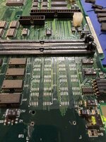
I got it reinstalled, and repairs two traces that were damaged, and still wasn’t able to get a boot chime. That’s when I realized the board was missing some chips that were there on my other Q650 / Q800 board. U18 and U22 were removed from the board. As was RP7. So I pulled the chips from another battery bombed board and was able to get a boot chime, followed by a sad Mac. Some of the memory chips near the battery looked a bit suspect, so I removed one of the banks of memory chips, U44, u45, U49, U50, U53, U54, U60, and U61. I cleaned and tested the traces I could see and they seemed good. And I got a boot chime and no sad Mac. I also got video out, but it was corrupt.

it seems like I’ve lost some colors, or the colors are scrambled. I have a green mouse, and vertical pink dotted lines down the screen. This doesn’t change with putting in known good vram chips installed or not

IMG_8494.jpeg


The other issue is that I obviously have half the built in memory with the chips I removed. I can out ram sticks in slots 1 and 3 and they work great. But if I RAM in slot 2 or 4, the sad Mac chime returns. Did I miss a damaged trace for slot 2/4 or will it not work with the on board RAM chips missing?

Other things seem to work fine. my ADB mouse works when plugged and I was able to boot from a BlueSCSI.

Where else do I need to look around for the corrupt video issue? Should I be concerned that the chips were slightly different for U18 / U22? They were still F245 chips. Just seemed to be Motorola branded. Also, the resistor pack at RP7 was a bit different, but I’m wondering if the 9247 vs 9316 markings were a date code? 1992 or 1993 would make sense for these, I think. All the chips that I believe are on board video ram (U20-U32) seem to be in good shape as do the traces nearby.

Appreciate any help or insight yall can provide!
IMG_8491.jpegIMG_8498.jpegIMG_8501.jpeg
 

Attachments

  • IMG_8486.jpeg
    IMG_8486.jpeg
    1.9 MB · Views: 20

wottle

Active Tinkerer
Oct 30, 2021
800
547
93
48
Fort Mill, SC
Awesome. I’ll take a look at that and see if maybe there is an issue with any of the traces. Would a bad on board memory chip cause this behavior? I have a couple dead boards that I could swap in chips from.
Alternatively, would it work if I removed all 4 chips from the board and just used the vram SIMMs (assuming the traces are all good)?
 

iigs123

New Tinkerer
Oct 13, 2025
12
5
3
If I were you I'd check all the traces first before trying to remove any components. I suppose bad VRAM could cause it. I don't know if it would work without onboard VRAM.

I fixed an LC II recently that had kinda similar video issues, and it was strictly a couple of broken traces between the VRAM and CLUT chip. Actually the "break" was really hidden as no visible damage was on the motherboard.


I also fixed up a Q610 by replacing an F245 that was eaten. It got it to boot and generally works fine, although I'm still hunting down a problem that seems isolated to the VRAM SIMMs. I believe, but i'm not certain, that the purpose of those bus transceivers is to handle the "general" data bus so if one was bad or out of spec the machine probably wouldn't boot at all, or would crash pretty quickly.
 
  • Like
Reactions: wottle

wottle

Active Tinkerer
Oct 30, 2021
800
547
93
48
Fort Mill, SC
I also fixed up a Q610 by replacing an F245 that was eaten. It got it to boot and generally works fine, although I'm still hunting down a problem that seems isolated to the VRAM SIMMs. I believe, but i'm not certain, that the purpose of those bus transceivers is to handle the "general" data bus so if one was bad or out of spec the machine probably wouldn't boot at all, or would crash pretty quickly.
The 650 definitely wouldn’t boot with two of the F245s removed! I’ll try to run through the traces tonight. Thanks!
 

joevt

Tinkerer
Mar 5, 2023
190
68
28
What color depth is being used in the photo? Change it to B&W so we can see which VRAM data lines are broken.
 

wottle

Active Tinkerer
Oct 30, 2021
800
547
93
48
Fort Mill, SC
What color depth is being used in the photo? Change it to B&W so we can see which VRAM data lines are broken.
It was set to 256 colors. I did change it to thousands of colors and to grayscale to see it if got better, but it didn’t seem to. I didn’t think to change it to B&W, but I’ll do that tonight and see how it looks.
 

wottle

Active Tinkerer
Oct 30, 2021
800
547
93
48
Fort Mill, SC
Ok, as I was looking at the traces in that area, I realized there was another chip that wasn’t populated on the board, U3, right by the video output. I was hoping that was the cause of the problem. I grabbed it off of my spare board and started it up again but the video was still bad, although now somewhat different.

It seems like the corruption is closer spaced the more colors I have (which in my mind with little understanding of how this works seems like it points to some part of the memory being bad opposite. If a certain memory line was bad, e.g. every 8th bit was bad, the higher color depth mean the corruption would be more condensed?).
Anyway, when I have thousands of colors, the repetitive pattern is essentially gone.

black and white:
IMG_8515.jpeg


16 colors:
IMG_8520.jpeg


256 colors:
IMG_8521.jpeg


Thousands of colors:
IMG_8518.jpeg

Thousands of colors with a gradient background:

IMG_8522.jpeg

Another thing of note is that when the machine boots (256 colors), it seems like any white areas have pink pinstripes. But light gray areas do not.
IMG_8517.jpeg


I tried reading the schematic that was sent but either I am not reading it properly or the 650 is too different. It does also appear many of the lines from the 343S1091-A chip go to nearby RC3-RC6 chips. All those traces tested good.

Does this help narrow things down?
 

iigs123

New Tinkerer
Oct 13, 2025
12
5
3
I forgot about the RC chips. You should be able to see continuity from the Antelope CLUT chip PD[0] - PD[31] pins over to an adjacent resistor chip, and then from the other side of the resistor chip to the VRAM slot. Or from CLUT to VRAM with some resistance.


For the pinout of the CLUT chip see PDF page 8/14 of the LC475 schematic.

For the pinout of the VRAM slot see PDF page 6/14 of the LC475 schematic.


For example PD[0] is pin 11 on the CLUT, and pin 71 on the VRAM. The VRAM SIMMS are 68 pins, so pin 71 is actually in the 2nd slot.

You might need a bodge from the VRAM over to the resitor chip next to the CLUT.
 
  • Like
Reactions: wottle

wottle

Active Tinkerer
Oct 30, 2021
800
547
93
48
Fort Mill, SC
The B&W image indicates a 32-bit bus with D29 or D28 being stuck low.
I forgot about the RC chips. You should be able to see continuity from the Antelope CLUT chip PD[0] - PD[31] pins over to an adjacent resistor chip, and then from the other side of the resistor chip to the VRAM slot. Or from CLUT to VRAM with some resistance.


For the pinout of the CLUT chip see PDF page 8/14 of the LC475 schematic.

For the pinout of the VRAM slot see PDF page 6/14 of the LC475 schematic.


For example PD[0] is pin 11 on the CLUT, and pin 71 on the VRAM. The VRAM SIMMS are 68 pins, so pin 71 is actually in the 2nd slot.

You might need a bodge from the VRAM over to the resitor chip next to the CLUT.
I traced the PD[28] and PD[29] to the VRAM. all looks good - it does have a resistor inline, but that also seems ok. @joevt is D29 / D28 different than the PD28 and PD29 I looked at?
 

joevt

Tinkerer
Mar 5, 2023
190
68
28
I traced the PD[28] and PD[29] to the VRAM. all looks good - it does have a resistor inline, but that also seems ok. @joevt is D29 / D28 different than the PD28 and PD29 I looked at?
I would have to look at a schematic to know the actual names of the signals/traces.

Can you take a screenshot? If the problem is not captured in the screen shot, then the problem is not between the CPU and the VRAM or in the VRAM - it is between the VRAM and the display output.
 

wottle

Active Tinkerer
Oct 30, 2021
800
547
93
48
Fort Mill, SC
I would have to look at a schematic to know the actual names of the signals/traces.

Can you take a screenshot? If the problem is not captured in the screen shot, then the problem is not between the CPU and the VRAM or in the VRAM - it is between the VRAM and the display output.
I didn’t think about doing screenshot. I assumed it was something on the output side.
IMG_8530.jpeg

Since the lines show up in the screenshot, this means it’s between the CPU and the vram (or the vram itself)?

Also, after checking some of the traces last night and not finding anything, I started to suspect maybe U8 was bad, so I swapped it with one from another board. No change in behavior.

Really appreciate all the help. I’ve got no background in EE so reading schematics isn’t my strength.
 

wottle

Active Tinkerer
Oct 30, 2021
800
547
93
48
Fort Mill, SC

wottle

Active Tinkerer
Oct 30, 2021
800
547
93
48
Fort Mill, SC
OK, so I did some probing with the Q800 schematics and checked some additional things. I have been focused on anything related to D28/D29.

For PDf[28] and PDf[29] and PD[28] and PD[29]:

Starting at U8, the connection from 60 and 56 to RC4 15 and 19 are good. The resistance across RC4 pins 15 and 19 to pins 6 and 2 is 51ohms. I have good connection from RC4 pins 6 and 2 to pins 36 and 37 on U20, as well as the VRAM SIMM slot one at pins 55 and 56.

For D[28] and D[29] (not sure if they are related, but I checked them):

Starting at the CPU, I tested good connectivity between the CPU at C18 and E16 to U19 at pins 14 and 13, and J18 at pins 92 and 21.

For BDb[28/29]:
Good connectivity from U19 pins 6 and 7 to U20 pins 31 and 32, as well as RP6 pins 2 and 1 and J19 pins 58 and 59.

For BDa[28/29]:
Good connectivity from U18 pins 6 and 7 to RP9 pins 2 and 1 and J24 pins 59 and 60.

I also tried swapping out the U20 and CPU to no effect.

Any thoughts on where else I should look between the CPU and the VRAM or CLUT?
 

iigs123

New Tinkerer
Oct 13, 2025
12
5
3
It seems like it would be on the D[0]-D[31] side.

There are other video memory related signals that come out of the djMEMC chip you could check. VRAS0, VCAS0, TROE0, DSF0 and more. These go thru resistors before going to the memory chips.

In the past I've created an excel spreadsheet to track what traces I've tested, to where. It is very tedious work!