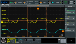
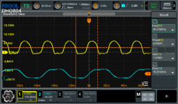
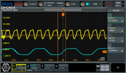
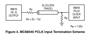
As I mentioned earlier in this thread, there are TERMINATION RESISTORS used on the 2X_Q output of the 88916DW chip, which leads to PCLK on the 68040 CPU. So for example, when the CPU clock speed is 33MHz, PCLK will be twice that at 66MHz. And that is really the reason the 88916 chip is used -- to provide multiple clocks.
But I can't quite figure out Apple's termination scheme.
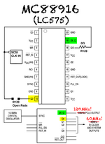
This is from the LC575 schematic (gray parts are VERY HARD TO READ):
And this is from the Quadra 605 schematic (much easier to read):
So except for the Resistor number, the info in that little box toward the right seems to be the same for both motherboards.
Now the data sheet for the
MC88920 is exactly the same as the datasheet for the
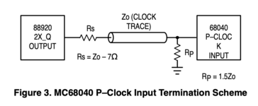
MC88916 when it comes to the FORMULA that let's you calculate the two resistances...


So if we examine those LC575 & Q605 schematics, we see the following:
Rs = 61.9Ω 1%
= Zo-7Ω (as per the datasheet)
And for a 33MHz CPU clock, we see this:
Rp = 140Ω 1%
= 1.5xZo (from datasheet)
So, what is Zo?
Using Rp=140Ω...
Zo = 140 / 1.5 = 93.33Ω
Therefore, Rs = 93.33-7 = 86.33Ω
But Rs = 61.9Ω!!!
Using Rp=110Ω...
110 / 1.5 = 73.33Ω
Therefore, Rs = 73.33-7 = 66.33Ω
But Rs = 61.9Ω!!!
Rs is a fixed 61.9Ω value.
And we know Zo=Rs+7Ω.
So Zo=61.9+7 = 68.9Ω
Therefore Rp=1.5Zo=103.35Ω
But that cannot be right because Zo will change according to the 2X_Q output clock frequency!
So the question is, what should Rp be for clock speeds higher than 40MHz?
I never changed Rs or Rp before, and I had been testing the full range of clock speeds from 33Mhz (stock) all the way to 50MHz (stable, but some freezing when booting 7.6.1 and 8.1 and even 7.5.5, although 7.1 always worked. But the fact remains we have a HF transmission line which requires proper termination via resistors, hence this is a valid question to ponder.
The 88920 datasheet has this Application Note pertaining to Termination of the 2X_Q output:
Two specs (tRISE/FALL and tPULSE Width 2X_Q output,
see AC Specifications) guarantee that the MC88920
meets the 20MHz and 25MHz 68040 P–Clock input
specification (at 40MHz and 50MHz). For these two specs
to be guaranteed by Motorola, the termination scheme
shown in Figure 3 must be used. For applications which
require 1.5V thresholds, but do not require a tight duty
cycle the Rp resistor can be ignored.
Bear in mind the 88920 chip is only rated for 25MHz CPU operation (50MHz on the 2X_Q output).
The 88916 datasheet has this Application Note pertaining to Termination of the 2X_Q output:
The pulse width spec for the Q and 2Q_X outputs is
referenced to a VCC/2 threshold. To translate this down
to a 1.5V reference with the same pulse width tolerance,
the termination scheme pictured in Figure 3 must be
used. This termination scheme is required to drive the
PCLK input of the 68040 microprocessor with the 88916
outputs.
The 88916DW80 allows for a CPU clock speed of 40MHz, which means 80MHz on the 2X_Q output.
Thoughts?