5v FPM DIMM's!

Kai Robinson

TinkerDifferent Board President 2023
Staff member
Founder
Sep 2, 2021
1,153
1
1,162
113
42
Worthing, UK
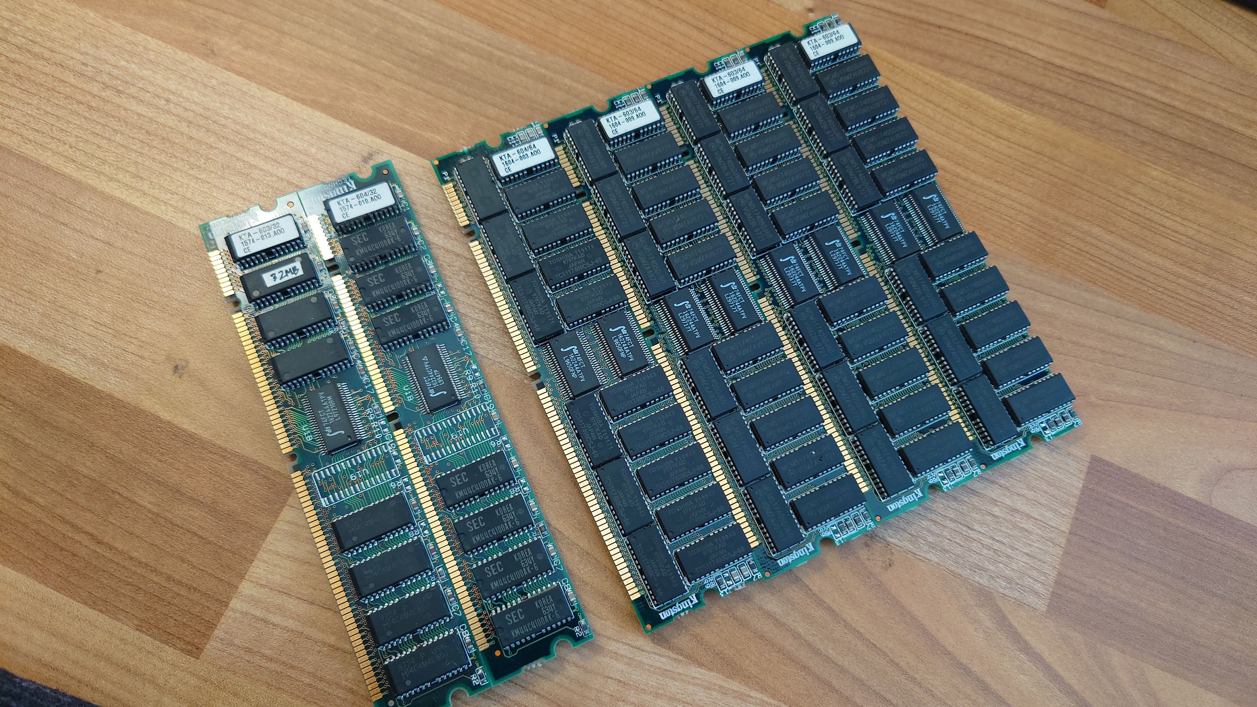
These are getting surprisingly harder to find. Seriously, this haul of 4x64MB and 2 x 32MB DIMM's cost more than a 32GB DDR4 kit... But it'll be worth it!

The extra 256MB is destined for my 9600, the other 64MB destined for the 7500.

@Zane Kaminski - reckon you could make these with more modern chips?

DSC_1080.JPG
 
  • Like
Reactions: Mr. Fahrenheit

trag

Tinkerer
Oct 25, 2021
270
128
43
It seems like most folks don't care for the PM7200 much, but one interesting thing about it is that according to the Hardware Developer Note, it can address 256MB DIMMs, meaning that the maxium capacity could be 1GB of RAM, if anyone ever built some 256MB DIMMs for it.

Non-EDO of course. :)

12 X 12 addressing and 13 X 11 addressing are supported and 2 banks per DIMM. So 2^24 addresses => 16M address X 8 bytes wide => 128MB X 2 Banks => 256MB.
 
  • Like
Reactions: Mr. Fahrenheit

Zane Kaminski

Administrator
Staff member
Founder
Sep 5, 2021
371
608
93
Columbus, Ohio, USA
I don’t think it can really be made with new chips. There are several issues....

For even 70ns FPM DRAM, the fast-page /CAS access time is quite short, 20ns or so. All you have to do to accomplish a fast-page access is to set up the column address on the DRAM address bus, assert /CAS, then wait 20ns for the read data to come back. There isn’t even any address-to-/CAS setup time so the whole thing occurs inside of 20ns.

Compare this to SDRAM, the go-to cheap RAM if you want tens of megabytes. Typically SDRAM systems run with a fixed-frequency clock. The lowest-latency way to use SDRAM is with CAS latency 2 at 133 MHz, making for a 7.5ns cycle time. So to read from an SDRAM given that the right row is already open (analogous to an FPM cycle), you have to issue a read command, wait 1.5 ns of setup time, bring clock high, wait 3.75 ns, bring clock low and issue a NOP command, wait 3.75 ns, bring clock high again, wait 5.4 ns, and then the data comes out.

So just in the SDRAM, 14.4ns of your 20 nanosecond budget is used up. In/out level shift delay can be minimized to a total of 0.5 ns using voltage-limiting FET switches, so then you have 5 nanoseconds to synchronize the /CAS signal. With a 7.5ns clock period, this is impossible! The 133 MHz clock would be running independently of the clock on the main board and it would be possible to just miss /CAS. Then you have to wait 7.5ns more and that blows the remaining 5ns budget. And realistically you need some additional fraction of a clock cycle of synchronization time budgeted.

So the lesson here is, it’s impossible to emulate 70ns FPM with SDRAM running from a repetitive clock. There is another solution though.

Instead of having the clock always running, in which case you can sort of get the “just missed it” slow alignment that can take up to one whole clock cycle, what you can do is generate clock pulses to the SDRAM just in response to /RAS and /CAS events from the host system. With this approach, you get the entire 5ns (not much though) to pay for your combinational delays generating the clock. The issue here is that to read (as well as to finish a write), you have to pulse the clock twice. Without a crystal controlled oscillator, it’s hard to get the exact 7.5ns delay in between clock pulses, and any variance there subtracts from the 5ns. Crystals can’t be run for just one clock cycle here and there; they take time to start oscillating. So you have to implement the delays with delay line traces on the PCB. A 7.5ns delay is about 50 inches of 50 ohm trace... but you can do it.

Alright, so you have your almost-no-delay FET switches doing the level shifting, you’ve built an ASIC that can put out the SDRAM command/address multiple time using only the five spare nanoseconds, your board has a hundred inches of delay lines, now what else has to be done to hook up SDRAM to an FPM/EDO bus?

Well, I don’t know how DRAM DIMMs are addressed, but with the kinds of DRAM chips used on 30-pin SIMMs, there is an array size mismatch between DRAM and SDRAM. What I mean is, a 16 MB 30-pin DRAM SIMM has 4096 rows and 4096 columns of 8 bits. That means when you have opened a given row, any of the 4096 bytes therein must be able to be accessed in 20ns. The largest SDRAM chips still made have only 1024 byte rows so you need four of them, totaling 64 or 128 megabytes just to make the 16 MB 30-pin SIMM. The old 512Mb SDRAMs had 2048 byte rows so you only need two but it’s still 128 MB required just to implement 16 MB. For the 64-bit DIMM you may need 8 or 16 SDRAM chips. (I dunno the typical row/column size for a 64 MB DIMM.)

So... FET switches, special ASIC that has pin-to-pin delays much much lower than 5ns (gotta incur it multiple times), big long delay lines, a bunch more SDRAM chips than you’d think are required... I’ll start tomorrow! Hahaha nooo

You could use SRAM but it’ll cost several hundred bucks for 64 MB. DDRx has worse latency than SDRAM although I think they did double the number of columns per row in DDR2 so you’d only need half the chips if you used DDR2, but the extra latency would certainly make it impossible to make the 70ns FPM access timing of 20ns. And going from 70ns to 60ns means you’ve gotta do a /CAS access in 16-18ns, so all but 1 or 3ns of the 5ns is gone.

Tough problem! I don’t think it will be solved until SRAM is cheap enough to build a tens of MB SIMM/DIMM/kit for tens of bucks.
 
Last edited:
  • Love
Reactions: Stephen

Kai Robinson

TinkerDifferent Board President 2023
Staff member
Founder
Sep 2, 2021
1,153
1
1,162
113
42
Worthing, UK
Well, I was thinking of using regular dram chips that are available in quantity, not necessarily sdram or sram.
 

Zane Kaminski

Administrator
Staff member
Founder
Sep 5, 2021
371
608
93
Columbus, Ohio, USA
Well, I was thinking of using regular dram chips that are available in quantity, not necessarily sdram or sram.
It’s doable but you need eight 8Mx8 chips to make one 64 MB DIMM which are kinda rare. It’s a lot of old pricey RAM. Consider that a 64 MB kit of four 16 MB 30-pin SIMMs is going for $45 and this is not too far above the chip cost. I think at GW we have been paying over $20 just for the chips to sell such a 64 MB kit at $45, then there’s the boards, shipping, etc. Unlike, for example, our Apple IIgs RAM, which nominally costs 1/3 the selling price, our SIMMs have a decidedly more “commodity” pricing style. It’s not clear that that many people wanna get into making DIMMs if the profit is so low. You could make just ten or so but then the costs might be higher than buying them. It works best to buy a bunch of chips at once, but there is little financial reward for such a large investment. If someone can uncover a big stash of 8Mx8 DRAMs for cheap then the decision to make 64 MB DIMMs is easy, but I don’t know that anyone will let those chips go for under $2-3, so that’s $16-24 of cost on a 64 MB DIMM not counting the board and other stuff. So I consider it to mainly be a logistical issue of finding a cheap source of the chips.

Anyone have any leads?
 

Zane Kaminski

Administrator
Staff member
Founder
Sep 5, 2021
371
608
93
Columbus, Ohio, USA
For DIMM's, would it not be best to use something like these: https://www.utsource.net/itm/p/11652925.html

1K refresh, 50ns 1Mx16 DRAM chips for $1.51 in 100 or more... And new, too.

I've always had good luck with the DRAM chips from utsource. Always arrived in oem packaging, too.
Issue is that it only makes an 8 MB DIMM, 16 MB if you do dual-sided placement and put eight on. So the chip cost is $12 for 16 MB and I think that’s above the market price for a 16 MB DIMM. You could put more DRAMs and further decode the /RAS or /CAS signals to get a larger SIMM but then you have a “composite SIMM” that loads the data bus too much by having more than one chip on the data bus per /RAS signal. Works okay on 68k Macs but the newer machines have tighter timings and the composite design sort of degrades the system timing margins, plus it would be $48 of chips for a 64 MB SIMM.

EDIT: What we want is like KM48C8100 (FPM) or KM48C8104 (EDO).
 
Last edited:

Kai Robinson

TinkerDifferent Board President 2023
Staff member
Founder
Sep 2, 2021
1,153
1
1,162
113
42
Worthing, UK

84cents each, but you'd need a buffer and a voltage regulator to step down from 5v to 3.3v

Perhaps the 74LVT162244 as the buffer?

Each chip is 8MB (64Mbit) in size, 8 chips needed for the full 64-bit data bus, which would also give you 64MB modules.

Call it 90 cents per DRAM chip, a buffer at 50 cents and a single regulator, you're looking at a chip cost of maybe $15? Plus PCB's for an extra $5 — that's a pretty reasonable price of $20 all in?
 
Last edited:

trag

Tinkerer
Oct 25, 2021
270
128
43
For DIMM's, would it not be best to use something like these: https://www.utsource.net/itm/p/11652925.html

1K refresh, 50ns 1Mx16 DRAM chips for $1.51 in 100 or more... And new, too.

I've always had good luck with the DRAM chips from utsource. Always arrived in oem packaging, too.

Those chips might be useful in adding the on-board memory back to the PM6500 though....

There was motherboard memory on the 6400, but Apple discarded it for the 6500, but left the pads on the board. I think that 1M X 16 is what's needed for those pads, but I'm not certain.
 

trag

Tinkerer
Oct 25, 2021
270
128
43

84cents each, but you'd need a buffer and a voltage regulator to step down from 5v to 3.3v
I've seen DIMMs for the X500/X600 built with 3.3V memory and there's no (additional) buffers. Just a 3.3V voltage regulator for the supply pins.

I've been meaning to track some of those down and take a closer look. There was some memory from Micron which ran on 3.3V but had 5V tolerant I/O. The Micron SRAM chips over in the caches thread are that type.
 

Zane Kaminski

Administrator
Staff member
Founder
Sep 5, 2021
371
608
93
Columbus, Ohio, USA

84cents each, but you'd need a buffer and a voltage regulator to step down from 5v to 3.3v

Perhaps the 74LVT162244 as the buffer?
Yes! LVT or LVC are fine for the address/control buffer. We need buffers on all the data lines too, so that’s 8 more LVC245s or whatever that are required. The 16244/16245 chips don’t really take any less space and aren’t a great value so I say let’s skip em and use two chips. With 8 data buffers on this thing, we may need to use the little QFN-20 packages for the ‘245s to keep the overall DIMM height short.

We need to think about the timing skew issue though. We will be buffering (to 3.3V) all the address and control lines so that’s roughly the same delay going to the DRAM as the buffers on a legacy buffered DIMM. But we are also putting buffers on the data bus (buffered DIMMs don’t do this) and so write data into the DIMM will be delayed compared to the control signals. Reads out of the DIMM will be similarly delayed, but the solution is easy—just put 50ns chips and spec the module at 60ns. But writes could be problematic if the system is using the DIMM with very little margin since the data input will be delayed compared to the write strobe and there could be a write-data-setup-to-/CAS timing violation. We have to decide whether to ignore this (maybe), employ < 1 ns delay FET switches (expensive), or double-buffer the address so the relative delay to the data is maintained (degrades speed performance).

We also need to implement the data bus direction control unless we are using FET switches (which solve the skew problem too but cost as much as the RAMs). This is a little tricky because the direction control is based on CAS, OE, and WE and there is a memory aspect not only with EDO but with FPM too. That is, if /WE is low when /CAS falls then the data buffer stays off even if /WE rises later with /CAS still low. (I think?) EDO has another similar thing—the data buffer stays on after /CAS rises until cleared by a high level on /RAS or /OE inactive. If we are doing a dual-/RAS DIMM then the data bus control is additionally complicated by the fact that we have to sort of do it for two sets of RAM behind the buffers (otherwise we have to have 16 data buffers on a dual-/RAS DIMM)
 
Last edited:

Zane Kaminski

Administrator
Staff member
Founder
Sep 5, 2021
371
608
93
Columbus, Ohio, USA
I've seen DIMMs for the X500/X600 built with 3.3V memory and there's no (additional) buffers. Just a 3.3V voltage regulator for the supply pins.

I've been meaning to track some of those down and take a closer look. There was some memory from Micron which ran on 3.3V but had 5V tolerant I/O. The Micron SRAM chips over in the caches thread are that type.
Yeah it would be better to use the 5V-tolerant 3.3V stuff, then we could eliminate the eight data buffers and all the ugly control stuff but it’s only certain mask revisions that are 5V-tolerant. It’s hard to make sure you’re getting those.

But like I said before, $25 each is a hard price to beat! Seems like with just the RAMs and board we’re at $8, more if you consider the inevitable production scrap overhead. So we’re already in the realm of either commodity-type margins for the manufacturer or unusually high prices charged to the customer for like a “bespoke” product.
 

trag

Tinkerer
Oct 25, 2021
270
128
43
@Zane Kaminski So, I was looking at some of the level shifter chips. And they appear to convert 5V+ to Vcc (3.3V in this case), but in the other direction, the 3.3V outputs just go out as 3.3V to the 5V side. I'm guessing it doesn't matter because 3.3V is still high enough to register as a logical high level?

That's poorly worded, but it's meant to be a question.

I ought to list the actual part numbers, but I was looking on a different computer. I need to start keeping my datasheet collection in some web space so I can access all of them everywhere, instead of having six different collections.
 

trag

Tinkerer
Oct 25, 2021
270
128
43
Yeah it would be better to use the 5V-tolerant 3.3V stuff, then we could eliminate the eight data buffers and all the ugly control stuff but it’s only certain mask revisions that are 5V-tolerant. It’s hard to make sure you’re getting those.

The thing is, I'm not sure the memory chips they used actually were 5V tolerant on the IOs. It makes me wonder about what levels the X500 and X600 are actually using. Or the memory maker could have just been crossing their fingers that the memory chips wouldn't blow out before they closed up shop and disappeared.

That's why I want to find them and check the chip numbers.
 

Zane Kaminski

Administrator
Staff member
Founder
Sep 5, 2021
371
608
93
Columbus, Ohio, USA
Or the memory maker could have just been crossing their fingers that the memory chips wouldn't blow out before they closed up shop and disappeared.
Yes it’s a bit of this but also there are legit 5V tolerant 3.3V DRAMs. The difference between a 5V tolerant 3.3V DRAM and one that's not is in the input protection circuit. The "classic CMOS" protection circuit is employed on a chip is a set of diodes sort of from ground to the pin and from the pin to Vcc. Thus input signals beyond the supply rails are clamped. Here's a picture:
1635748575822.png


Of course, if Vcc is 3V and you apply a 5V signal to the pin, the 5V signal sort of gets shorted to the 3V Vcc through the ESD diode. This in and of itself is not necessarily bad. If you check the datasheet for 74HC-series logic, you see that they support +/- 25 mA of clamp current. So with this setup you can do input level translation by putting the right size of resistor in series with the pin to limit the clamp current to acceptable levels. Check this picture from the Altera MAX II datasheet:
1635748924904.png


Now, there are some problems with this approach. Firstly, I don't think you're supposed to do it with DRAMs. You've gotta keep to the clamp current spec in the datasheet and if it's not listed then don't try this approach. To keep the clamp current reasonable, the resistor has to be in the range of 100-1000 ohms. If you have a 10 pF input, 1000 ohms adds an extra ~10ns propagation delay going in. Going out is even worse. Imagine you're trying to drive a 100 pF bus (not even that much). 1000 ohms adds 100ns delay. So this approach is only good for slowish inputs, not bidirectional signals like a RAM data bus.

So some chips have a different ESD diode approach. The key issue with the previous approach is the clamp current. To address this, some ICs stack several protection diodes going to Vcc. Therefore the pin only clamps when the input is multiple diode drops above Vcc and thus a chip powered at 3.3V can have 5V signals applied without clamping. Or the upper clamp is removed and the lower clamp diode is replaced with something along the lines of a zener, with a controlled reverse breakdown voltage above 5V.

This is the approach used by the few 5V-tolerant 3V DRAMs. Advantage is that you can just directly connect them to a 5V bus. Since most 5V chips work with TTL-level inputs where < 0.8V is a 0 and > 2.0V is a 1, the 5V TTL thresholds basically line up perfectly with a 3V CMOS chip whose outputs go nearly to the rails when unloaded. So no problem with the 5V chips understanding the 3V logic.

The problem is, as usual, a parts supply thing. We can make the board, put the 3V regulator on, etc., but it may be difficult to source chips that are actually 5V tolerant and we can be sure of it. Lemme illustrate my point.

This is from the datasheet for the KM48V8100B, an 8Mx8 FPM DRAM. Notice in recommended operating conditions, max input voltage is 5.5V or 6.5V for short pulse widths:
1635749812699.png


Now from the KM48V8100C datasheet... same chip, just revision C, right? Nope, max input voltage is Vcc+0.3 (indicating the presence of the upper clamp diode):
1635749922373.png


So it's hard to get the right chips. Remanufactured ICs are a no-no, because who can say whether they're actually the revision claimed? Everyone just sort of ignores the revision letter at the end of the part number because they're seen as basically interchangeable.

Now I had an interesting experience that led me to discover all this. I bought like 10 72-pin SIMMs on eBay. All had remanufactured Micron chips. The datasheet for the part numbers on the chips suggested they weren't 5V tolerant and had the clamp diodes. But then I did an input clamp current test and could detect absolutely no difference in input current as the pin went above 3.3V. For a 5V CMOS DRAM, taking the pin more than 1V above Vcc would certainly cause a bunch of input current through the ESD diode. So were the chips mislabeled and actually 5V tolerant? Was Micron being conservative, or did they attempt to engineer 5V tolerance into their chips but were not successful enough to spec it? Who knows...
 
  • Love
Reactions: alxlab

trag

Tinkerer
Oct 25, 2021
270
128
43
@Zane Kaminski Thank you for the detailed explanation. I always appreciate the effort you put into education.

I also really appreciated the explanation of bus timing for caches on the IIci that you posted a while back but I think that was lost in the great M68kmla fire of '21...

I had not thought in terms of clamping diodes for this application -- although I was just discussing with a coworker whether they had blown a component by reverse biasing it and mentioned it might have been protected by clamping diodes. I can know about a thing and still not think to apply it everywhere...

I just saw an interesting thing on Ebay. Sets of four 64MB 72-pin SIMMs. https://www.ebay.com/itm/124443425895

They appear to be built out of a Micron MT4LC16M4H9 chips, which are 3.3V supply. Then buried in Note 26 is this:

26. VIH overshoot: VIH (MAX) = VCC + 2V for a pulse
width £ 10ns, and the pulse width cannot be
greater than one third of the cycle rate. VIL
undershoot: VIL (MIN) = -2V for a pulse width £
10ns, and the pulse width cannot be greater than
one third of the cycle rate.

Which is pretty much what you were showing on the B revision above, I guess. Is that time period for the overshoot a breakdown/reaction time for the clamping diode (perhaps the reverse biased zener?) do you think?

P. S. Did you also post a scheme for preventing EDO from acting as EDO memory, basically making it behave like FPM? I was wondering if that would avoid whatever hazard the PM7200 has with EDO memory. It's a silly lark, but I really want to try building a 256MB DIMM for the 7200 one of these days. Being able to use EDO would make it easier, parts-wise.
 

Attachments

  • MT4LC16M4.pdf
    386.2 KB · Views: 150

Zane Kaminski

Administrator
Staff member
Founder
Sep 5, 2021
371
608
93
Columbus, Ohio, USA
Yep, that's the vendor I was referring to.

As for the overshoot, I think it's more of a thermal thing. If you've raised up the pin to Vcc+2V or whatever then there's a lot of current flowing and so the ESD diode on the die is heating up a lot.

About the EDO-to-FPM conversion, it's easier with 30-pin SIMMs but you can do it with 72-pin SIMMs and DIMMs too. The buffered aspect helps a lot.

The only difference between an EDO and FPM RAM is when the output buffer turns off during a read operation. The issue with FPM that prompted EDO is sort of a pipelining problem. To do a fast-page access, you bring /CAS low, wait 20ns or whatever for the data to come out, but then you have to wait additional time for the data to propagate through your system to the CPU or whatever. During this time, you can't bring /CAS high again for the requisite 10ns or so to prepare for another access. So in EDO, the output buffer turns on when you bring /CAS low to do a read as in FPM but stays on after /CAS rises. Therefore you can do a really narrow /CAS pulse width and bring /CAS high in preparation for the next access while the data is propagating through your system. Bringing /RAS or /OE high turns the output buffers off.

On a 30-pin SIMM, /OE is not pinned out to the SIMM connector and is just tied low. Instead you can connect /OE to /CAS and therefore the data out buffers are disabled at the end of the /CAS pulse and not "extended." So the RAM acts like FPM. Only 4-bit RAM chips have /OE or EDO, so doing this on a 30-pin SIMM implies you are doing a 2/3-chip SIMM and so the extra connections to /CAS increase the overall /CAS loading from 2 chips to 4, still within the 8-chip limit. We have been shipping SIMMs like this at Garrett's Workshop for some time with no issues. It just works!

On 72-pin SIMMs and DIMMs the /OE pin of the RAM chips goes to the connector so you can't just tie /OE to /CAS since then what do you do with the /OE input to the SIMM? So instead you OR them and send that to the DRAMs. Thus /OE to the chips is only low when both /OE and /CAS at the SIMM/DIMM edge are low. This gate delay subtracts from your timing if you are using an unbuffered SIMM but the buffer delay in a buffered SIMM/DIMM can be spent on the gate delay instead so there is no timing impact on a buffered RAM stick. Fortunately even if you do this on an unbuffered RAM, it just adds /CAS access time, whereas gating any of the control signals but /OE sort of unaligns the timing between RAS, CAS, WE, address, and write data.
 

trag

Tinkerer
Oct 25, 2021
270
128
43
So I was pondering the EDO vs. FPM scheme with /OE. And it occurred to me, why not apply that at the Motherboard of the 7200 instead of on just a few DIMMs?

But then I remembered that there are multiple /CAS lines to the DIMM. I need to check the pinout for 168 pin DIMMs again, but I'm about to go to bed, and I don't want to wake myself up that much. But I wanted to vomit forth my thoughts before I forget.

I know on 72 pin SIMMs there are four /CAS lines. I can't remember how many /OE lines there are, though. One? So if you tried to do that at the Motherboard level on a machine that uses 72 pin SIMMs, you'd be holding /OE high whenever anything less than a word-wise access was attempted.

That is, the motherboard tries to read a subset of the full 32 bit width, so some of the /CAS go low to perform teh operation. And /OE is low because that's necessary to enable the output. But some of the /CAS are high, because those parts of the 32 bits aren't being read. With /CAS OR'd to the single /OE, that means that /OE would be high if any /CAS was high and no data would be output from any of the memory. So nothing less than a full width access would be possible.

Probably the same on 168 pin DIMMs too.

So the only way to implement it is on individual DIMMs, not on the motherboard, and give every group of chips on a given /CAS line it's own OR gate operating on its /CAS line and the /OE line and feeding those chips' /OE pin(s).

Unless there's more than one /OE on DIMMs.

I guess I should check the Hardware Developer Notes too and see if they ever mention if the memory controllers support less than full width reads. Some memory controllers just read the full width and discard the unnecessary portions when they receive a partial-width read request.

It sure would be nice to cut a few traces (or uninstall a few resistors), add some OR gates and make PM7200 immune from EDO harm.

Hmmm. I with I had a PowerComputing Catalyst based machine on hand. They claimed that while they didn't support EDO memory, their implementation was not in danger of harm from EDO memory. They didn't change the Apple chipset. As far as I can tell, PCC didn't design any of their own chips. So what did they change?

Still leaves open the question of the mechanism of harm when one installs EDO in a 7200.

@Zane Kaminski Do you think the mechanism is that EDO memory in the 7200 outputs data when it is unexpected and can cause bus contention (more than one driver on the bus at a time) with the other motherboard chips? Perhaps the 7200 memory controller isn't very polite about disabling /OE on the memory because the designers assumed /CAS would take care of it for them?
 

Zane Kaminski

Administrator
Staff member
Founder
Sep 5, 2021
371
608
93
Columbus, Ohio, USA
Oops, forgot to respond to this.

Yeah, the issue is with chipsets that leave a row open (i.e. /RAS asserted) and then let the CPU access other devices. On the SE/30, for example, you can put EDO RAM in with no problem. (Not that anyone really makes 30-pin EDO SIMMs.) The chipset always brings /RAS high at the end of an /AS cycle so there's no concern about bus contention on subsequent accesses. More modern machines try to leave the rows open because of the increasing CPU-memory speed gap.

But the "harm" is just bus contention. Rarely damaging unless you let it go on for a long time. But of course the system won't work right with bus contention going on--data bus gets jumbled up and also the current flow, while not necessarily damaging, can sometimes cause ground bounce on daughterboard connectors. Suddenly a bunch of current flows because of the bus contention and the ground gets raised up. Systems like Apple II are particularly susceptible to this since there's only one ground pin and the inductance is fairly high when measured between the ground on one end of the card and the signal pins on the opposite end. So you try to stuff a bunch of current into the ground quickly and the card's ground gets raised up. At the same time, the power sort of browns out for the same reason. All this can conspire to make logic on the daughtercard think (for example) that /RESET is low and then part of the system resets and everything crashes. That's basically the most common short-term problem caused by bus contention, I think. Of course there's no /RESET on a RAM card but obviously bus contention should be avoided, even during times where there is no functional problem, per se.

About the read width, I think the cache system wants the whole data bus output for reads, so the chipset will assert /CAS for all the bytes during a read operation. That was the standard on MC68020+ and it oughta be the same on PPC. So for eight bytes, you have eight OR gates, each getting one of the /CAS signals plus the single card /OE. Each OR gate output goes to the /OE for the chip(s) providing the corresponding byte. So just like you said. DIMMs have two /OEs, I think, but they are for the front and back sides for a multi-rank/multi-RAS DIMM so the two /OEs correspond to two /RASs (one for each side).
 
Last edited:
  • Like
Reactions: trag