

I'm working on restoring a Performa 575, and, as usual, things started with a recap. The board was not battery bombed, but it was close... clearly bad chemicals had been wafting from the battery, and corrosion had impacted the board. I started the recap with hot tweezers before switching back to the clip and clean method. I am now frustrated with myself, because I abandoned the tweezers after lifting a trace.
I lifted the positive pad of C16, which is near the main logic board connector. This is my first time working on a 575 or any of its siblings. I'm a confused how the pad was connected. It looks like the pad is isolated from the copper, with the dark lines being nothing instead of traces. This "reverse mask" is confusing me.
Is that supposed to be a via on the top right side of the pad, or maybe one on the diagonal of the top left? I've picked at it some, but I'd prefer not to mess up too much of the solder mask without knowing what I'm looking for.
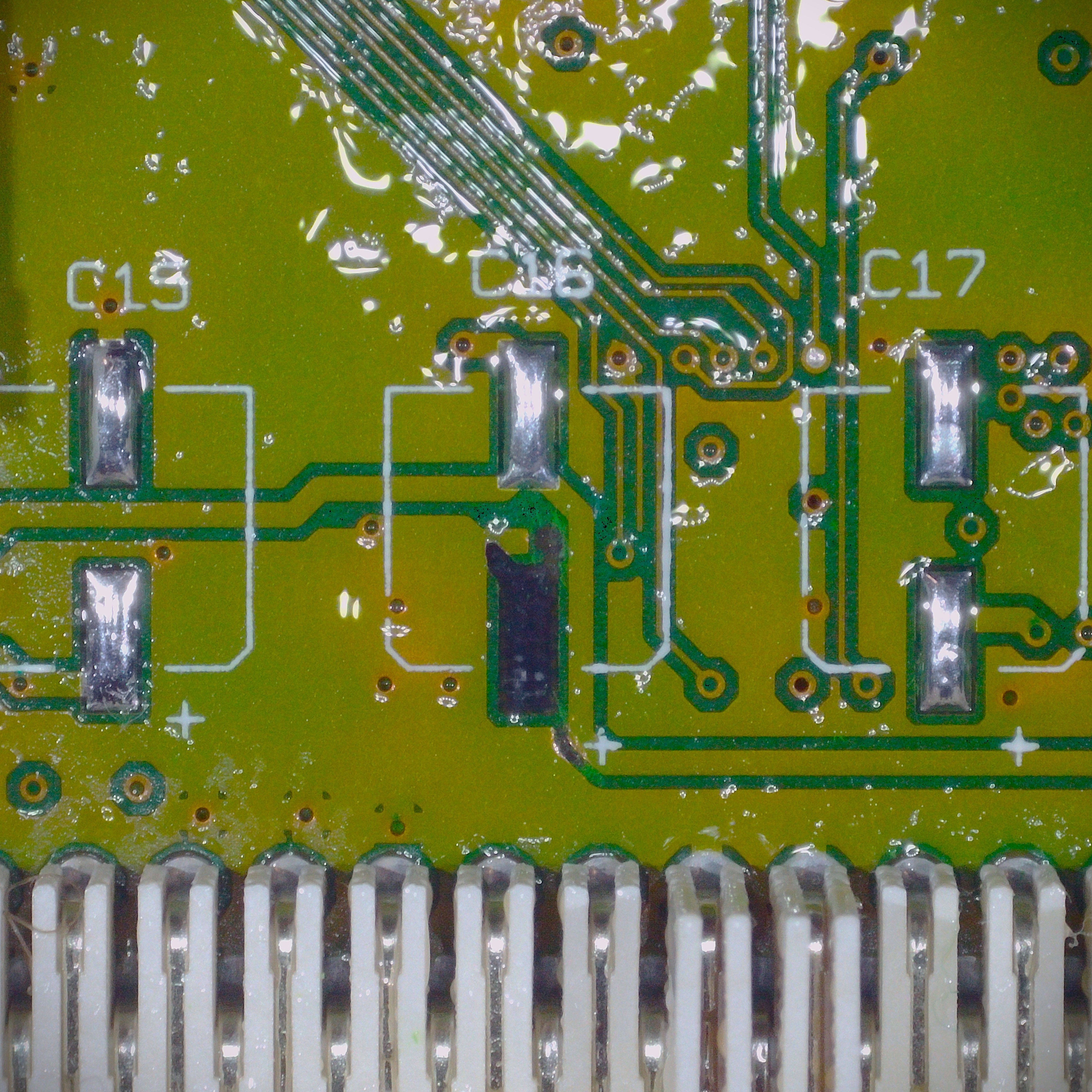
I lifted the positive pad of C16, which is near the main logic board connector. This is my first time working on a 575 or any of its siblings. I'm a confused how the pad was connected. It looks like the pad is isolated from the copper, with the dark lines being nothing instead of traces. This "reverse mask" is confusing me.
Is that supposed to be a via on the top right side of the pad, or maybe one on the diagonal of the top left? I've picked at it some, but I'd prefer not to mess up too much of the solder mask without knowing what I'm looking for.

