Recreating the Mac's CUDA / EGRET microcontroller chips - can it be done?

RetroViator

Tinkerer
Oct 30, 2021
83
104
33
retroviator.com
DosFox finally took the plunge and bought NOS chips, programmed them with the dumps and they do work. He has not provided any more details outside of that yet. Tons of NOS chips are available on ebay, but theres several variations.

The specific IC variation has not as of yet been reported.

I also saw he had to make a custom programmer to burn the PROM.

But, there is progress being made!
He shared that he was using a 68hc705e1– an EPROM variant of the original IC.

This link may be helpful: https://github.com/DosFox1/Raven-Programmer

I believe he was working with @max1zzz to test the results. I pointed him toward this thread. Perhaps he will jump into the discussion.
 
Last edited:
  • Like
Reactions: techknight

trag

Tinkerer
Oct 25, 2021
280
133
43
He shared that he was using a 68hc705e1– an EPROM variant of the original IC.

The tricky part in finding the part is finding a '705 with enough RAM. The e1 has 368 bytes of RAM. Most of the other variants have 176 or similarly small amounts.
 

Attachments

  • HC05E1GRS.pdf
    1 MB · Views: 15

techknight

Moderator
Staff member
Dec 2, 2021
73
78
18
North Carolina
He shared that he was using a 68hc705e1– an EPROM variant of the original IC.

This link may be helpful: https://github.com/DosFox1/Raven-Programmer

I believe he was working with @max1zzz to test the results. I pointed him toward this thread. Perhaps he will jump into the discussion.

I picked up a set of those chips from the Poland auction just to have them on hand for later. I will need to build a programmer eventually.
 
  • Like
Reactions: RetroViator

mmu_man

Tinkerer
Jan 30, 2022
160
85
28
It's not the only one that might work. I've been on that for 3 years :p
Which is why I didn't go the simple programmer route because they all have their own variant and I didn't want to make 3 different boards.
I have a prototype programmer already but the software is not yet working.
 
Last edited:
  • Love
Reactions: Mac84

DosFox

New Tinkerer
Dec 3, 2022
15
9
3
Hey all!
I was poked by @Kai Robinson and @bakkus to do a bit more of a write up/explanation of what the hell I managed to do! [Wow I rambled for a bit]

Bottom line is - we are able to make new CUDAs and EGRETs using 68HC705e1s.

I'm lead to believe in the vast majority of the cases the CUDA and EGRET as used on quite a few macintoshes is in reality a 68HC05e1 - and not any other variant of the 68HC05.
I'm lead to believe that due to two factors:
> The first is that the pinouts of the 68HC05e1 (hence referred to as the 'e1, as I'm probably going to strain my wrists typing "68HC05e1" every time) match the pinout of the EGRET/CUDA whenever they appear on schematics. The 68HC05e1 Datasheet is here.

1730637366070.png


> The second smoking gun is that all of the dumps of the EGRET/CUDA ROM are specifically 4352 bytes in size. These dumps can be accessed from the internet archive here.
The reason why 4352 is a bit of a magic number is because this is the total of the program data (4096 bytes) plus the user ROM vectors (16 bytes, also why the ROM size is sometimes counted as 4112 bytes), plus 240 bytes for the Bootloader.
As such, if the pinout matches, and the ROM dump matches - I would say with some confidence that both the EGRET and CUDA are both* 68HC05e1s.

EDIT
> Third reason, the pinouts are described in this Google Doc, they are all 68HC05e1s! This project tackles the parts that are listed in that directory, which pretty much describes most of the EGRETs/CUDAs.

*in most cases. As I found out, the CUDA Lite on the 4400 and Tanzania clones (umax, motorola etc), used in some cases a 68HC[7]05e5. The main difference between an 'e1 and a 'e5 is that the 'e5 has a bit more EPROM space. EPROM total is 5120 bytes instead of 4112. I have asked @Mac84 to dump any CUDA Lites he can, so we can compare the two. The program that was used to dump all of the EGRET/CUDA ROMs is this one from Mini vMac. Damn useful!

So we know that the EGRET/CUDA is likely a 68hc05e1 - which is slightly problematic as the program ROM and all accompanying data is stored in a Mask ROM - I.E, burnt by Motorola during manufacturing.

However, the 68HC05e1 has a relative - the 68HC705e1.
This is basically the exact same chip (same pinout, memory map and so on), except that the program ROM isn't a Mask ROM - it's an EPROM. We can program it!

Better yet, the datasheet included a full schematic and explanation of how to build a programmer to actually program them! (which uses an external 8k EPROM. Don't ask) There are two datasheets available for the 68HC705e1 - the first is from NXP (here), and it's a bit terrible as the programmer schematic isn't complete. The original Motorola one is a bit more accurate (here).

1730637410229.png


So we have a pretty good idea of what the original chip is, a good idea of what could be a drop in replacement, a programmer schematic as well as a good chunk of all of the ROMs we need to start programming EGRETs!

There is however, a few snags.
The first - and it's a biggy - is the Mask Option Register (MOR). The MOR is a single byte at location 0x1F00 which is only present on the '705e1, and it's basically a few settings that would be programmed into the Mask itself during manufacturing. The '05e1 uses that region for a self test ROM, and as such, the MOR settings wouldn't be present in any of the dumps.

The MOR handles three things:
1) internal interrupt (0.25s, 0.5s or 1s)
2) whether the watchdog is enabled
3) whether an external IRQ is used.

Thankfully by checking Macintosh schematics we can clearly see that the external interrupt isn't used (it's pin 1, and it's always brought high - so as the IRQ is active low, we can tell that it's never used. So this can be set to 0.
The wonderful PhilPem was able to do a bit of a disassembly on the EGRET code, and at least for the 341S0851 (which is apparently the most compatible of the EGRETs), the watchdog isn't used - so that can be set to 0.
The final question was around the internal interrupt - which is always set to something. However, as the EGRET is used as an RTC - we guessed that a 1s internal interrupt is probably correct.
This meant that the MOR is set to... 0x00. It's cleared. In my own implementation I wrote 0x04 (it does the same thing as 0x00) just to make sure I had definitely set the MOR to *something*.


1730637485632.png


With the MOR out of the way, came the problem of getting the dumps in the right format.
Now this does sound a bit odd, but stay with me.
The dumps that are found online - as far as I can tell - start dumping from the internal memory of the CUDA/EGRET and keeps going until it reaches 0x1FFF. This means that it will happily pick up the data for the Bootloader/Self Test ROM as it goes along. It also means that the data is offset by 3072 bytes, as the programmer expects the program data to start at 0x0F00, whereas the dumps always start off at 0x00.

The easiest solution is just to add 3072 bytes of clear data at the start of the dump, which will get you a mostly valid ROM file. This will give you exactly 8k (8192 bytes) of data to be flashed to the external EPROM.
It's also good practise to clear out 0x1F01 through to 0x1FEF, so you don't accidentally wipe the bootloader (I don't think that can happen, but it might?). Then you can set the MOR byte at 0x1F00 (if it's anything different to 0x00), and check that there is data from 0x1FF0 through to 0x1FFF. These 16 bytes describe the before mentioned user vector EPROM bytes.

You might begin to notice that this method of formatting the ROM file looks very similar to the actual memory map of the 68HC705e1, and that's because.... yes. The external EPROM basically needs to match the actual memory map of the 68HC705e1. Which is fair play, it probably made writing the bootloader easier!


1730637540596.png


The final change to the ROM file before it can be flashed is to duplicate a single byte from 0x1000 to 0x000. This is because some of the. 68HC705e1s (including the batch I bought) have a minor issue with timings during programming. This is described in the errata sheet here.
After all that, we have a good EPROM image to be programmed for the programmer.

Granted, I know it's a bit frustrating that you have to program an EPROM just to then program the 68HC705e1 - but my mantra is to always at first make as few changes to a reference design as possible. If something goes wrong, it's more likely there is an issue with the reference design than your own work.

I'm also aware that it's a bit of a confusing mess. If you need clarification - please let me know!

After all that, thankfully building the programmer is the easy bit.

It's a relatively straightforward design using the aforementioned 8k EPROM of your choice, with an external 12 bit counter to handle the EPROM address lines.
I also intentionally kept the entire thing as Through Hole rather than SMD - keeps it nice and easy for other people if they want to build their own!

The current design is VDEV2 of the Raven Programmer (VDEV1 had issues introduced by the NXP datasheet. Basically the NXP datasheet missed out what you do with PB1, PB6 and PB7. These have been corrected in VDEV2. All of the parts are relatively easy to find, even the 68HC705e1s can be purchased on ebay for relatively cheap - although I'll imagine stocks of them are probably in short supply, so no hoarding. Please!

After that, it's just a case of flicking the switches to program (on, on) - giving it 5v to begin with, then giving it 16v for the programming voltage - and hitting reset!

As mentioned, @max1zzz graciously accepted my request to test these first batches of EGRETs.
It was their request for the 341S0851, as it is one of the more compatible EGRETs. If I remember correctly it can at the very least be dropped into the LC line, as well as the IIsi.

His testing happily confirmed that the EGRET is working. I know the video only shows that the system chimes, however, we have had full confirmation that the ADB ports work, the RTC also increments at the correct rate (so my MOR settings are correct!), the PRAM settings are stored, and as far as we can tell the interrupts to the CPU are working as expected. A Techstep tester also indicates that the EGRET is happy!

1730636323257.png
1730636300730.png


Admittedly, we do still need to check that the soft power works by dropping it into a iisi, however, I feel that as the soft power is just another IO pin on the EGRET, and as all other functionality is working as expected - it's likely the new EGRET is happy and healthy.

So where to go from here?

The next steps is to start testing more and more EGRET/CUDA replacements.
I started this entire journey off because I purchased a horribly overpriced colour classic that I was lead to believe was fully alive - but it turned up dead, mostly due to a dead EGRET, likely due to other cap leak related failures. Unfortunately as I have other commitments (work, life, retrofest, other sad and dead computers) it may be some time before I can test all of the EGRET/CUDA replacements.

My long term goal is to have all of the dumped EGRET/CUDAs (or at least enough dumped ones for the entire Macintosh line) in the correct format for the programmer, programmed to actual 68hc705s and tested. However this may take some time!

In the meantime, I have acquired a CUDA lite from a Tanzania Macintosh clone (same as the Power Mac 4400), and I've successfully transferred it to my own 4400. This is important as this CUDA Lite used a 68HC705e5 part (as mentioned), so that the MOR for the CUDA should be present and able to be read - meaning that at least the MOR setting would be accurate for the CUDAs. (They appear to use the IRQ line, so the CUDA should theoretically have a different MOR) - but currently the data appears to be inconclusive, as the MOR byte is again 0x00!

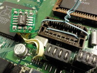
A zoomed in photo of a Macintosh 4400 logic board, showing an IC marked as 341S0285
The same area of the board, except that old IC has been replaced with a Motorola 68HC705


Either way - as mentioned, as all of the dumps present for the CUDAs and EGRETs are all 4352 bytes, they should all be theoretically compatible with the 68HC705e1. Therefore, all of the CUDAs and EGRETs should be able to be reproduced using this process, with the Raven Programmer.

TLDR; New EGRETs and CUDAs can be made with this (here) programmer and 68HC705e1 ICs, so long as the ROM is in the right format. 341S0851 EGRETs have been flashed and tested. CUDAs are a work in progress.

Also If you have any questions, either reply to me on here, I'm also on the Tinker Different Discord, as well as on Mastodon as DosFox (https://tech.lgbt/@DosFox). I'm aware this is a very long and complex subject, and I am atrocious at explaining things. If anyone needs any help (maybe a new EGRET or CUDA?) I'll be happy to help!


Also - Raven Programmer. This was a project for the spooky month of October. As an Egret is a bird, what's a spooky bird? Yep. A Raven. Gettit?
 
Last edited:

DosFox

New Tinkerer
Dec 3, 2022
15
9
3
It's not the only one that might work. I've been on that for 3 years :p
Which is why I didn't go the simple programmer route because they all have their own variant and I didn't want to make 3 different boards.
I have a prototype programmer already but the software is not yet working.
What is the other variant? I'm only aware of the EGRET/CUDA (68HC705e1) and the CUDA Lite (68HC705e5).

I'm more than happy to build two other programmers!
 

trag

Tinkerer
Oct 25, 2021
280
133
43
Then you can set the MOR byte to 0x1F00 (if it's anything different to 0x00),

Should the above have read: "Then you can set the MOR byte at 0x1F00 (if it's anything different to 0x00),


BTW, excellent posting. Thank you for the wonderful work.
 

DosFox

New Tinkerer
Dec 3, 2022
15
9
3
Should the above have read: "Then you can set the MOR byte at 0x1F00 (if it's anything different to 0x00),


BTW, excellent posting. Thank you for the wonderful work.
Hah thanks for catching the typo
 
  • Like
Reactions: trag

mmu_man

Tinkerer
Jan 30, 2022
160
85
28
When I say I'm on it… I'm on it.


EDIT
> Third reason, the pinouts are described in this Google Doc, they are all 68HC05e1s! This project tackles the parts that are listed in that directory, which pretty much describes most of the EGRETs/CUDAs.

I spent nights digging the schematics and comparing pinouts, and producing that spreadsheet, but you didn't ask :p

I also patched radare2 to fix support for 6805 disassembly so I could reverse the other dumps, but haven't finished yet. Fixing tools takes so much time…

Then I modded a recapped LCIII to add support back last December, after noticing they were just regular E1s with evolution of the same original code, and I knew there was an OTP version :

Mac_LCIII_DSCN2868.jpg


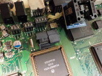
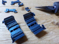
But the modified SOJ socket didn't make good contacts so I went for splicing the largest SOIC sockets I could find:

misc_DSCN2887.jpg
misc_DSCN2899.jpg


I also looked at the old Motorola catalogs to find possible compatible uCs because the E1 weren't easy to come by… Tekmos claimed to remake some but oddly never found any of those chips.

Screenshot_20241115_015236.png


What is the other variant? I'm only aware of the EGRET/CUDA (68HC705e1) and the CUDA Lite (68HC705e5).

I'm more than happy to build two other programmers!

So yes, actually the E5 is exactly the same as the E1 with just more RAM and EPROM. Sadly the E6 is much different, the I/O port registers differ already so you can't throw the same code in. And if the code is aligned properly the E1 one should run in the E5 if they are cheaper. The only concern could be the clock PLL, I don't remember verifying this.

The final question was around the internal interrupt - which is always set to something. However, as the EGRET is used as an RTC - we guessed that a 1s internal interrupt is probably correct.
Hadn't looked at it yet but I suppose so, in any case the clock would just skew quickly for other values.
3) whether an external IRQ is used.
Not exactly, it only specifies if it is detected on edges (when it gets low), or at the level (ie. triggered for as long as it's low). Bad setting here can cause an interrupt storm, or not detecting it properly.

It's also good practise to clear out 0x1F01 through to 0x1FEF, so you don't accidentally wipe the bootloader (I don't think that can happen, but it might?).
Dunno, but datasheet says blank state is 00 for the EPROM, so yeah.

Which is fair play, it probably made writing the bootloader easier!
But not a host programmer, specially when they don't tell how they handle byte 0. 🙃
Basically the NXP datasheet missed out what you do with PB1, PB6 and PB7.
Actually it does say what to do with PB1 in the text even if it's missing on the schematics. The other two are likely just ignored by the bootloader anyway.

The final change to the ROM file before it can be flashed is to duplicate a single byte from 0x1000 to 0x000. This is because some of the. 68HC705e1s (including the batch I bought) have a minor issue with timings during programming.
That's because they use a 12 bit counter and so they drive A12 directly… but they failed at it. Which is why for the E5 they changed the programmer circuit to make a flip-flop out of separate gates so they can set the bit earlier, because… just because. Yes I simulated them.

Which means you need a separate programmer just for this chip, in addition to burning EPROMs for each binary, which I found lame, which is why I didn't want to build these and instead pull my hair at using an Arduino. 😓

I already had this idea when I found a German forum mentioning a similar programmer for some PC clone keyboard controller chip. I created an account to download the code but it was quite basic and missed some parts, but at least shown it could work.

I spent months thinking about generating and switching VPP, because I wanted to support multiple chips, including the original HC05E1 which can be sent code to RAM so in theory could be dumped directly. And wondering about zener diodes, regulators and analog muxes… To later just go for an OpAmp as 5 times follower on a PWM output with a cap, which uses less GPIOs and works quite well when you use an amp that accepts 0V input (they are usually meant for symmetrical power and don't accept the full range on input). Which I stacked on the existing socket because at 2am you usually don't want to rewire the whole board, after burning two of them:

68HC705_DSCN3767.jpg


I recall spending way too much time in Fritzing for the 0120 test circuit, and also wasting time tring to design the prototype board part for it, so I just went for KiCad for the schematics, and placing the parts on the PCB, though I didn't route them yet as I wired them by hand for the prototype, not knowing if it'd work first hand. It didn't anyway, I had to change the design several times (had a transistor to pull VPP to ground through a resistor, but the chip took too much current so either VPP would be too low at the chip, or it wouldn't raise enough at the amp). Now it even monitors VPP and bails out if it can't get to it.

Screenshot_20241115_025233.png


KiCad can show a specific net over the PCB, making it much easier to verify you didn't miss a wire:

Screenshot_20241115_025449.png


I also tried several parts for the clock, turns out the 100nF on XFC is really needed; for days it wouldn't want to talk, then it would talk forever… I ended up synthesizing the clock from the Arduino as well, as it's totally capable of that, so less parts on the board, and you can tune it to slow it down for testing. Prototype has a jumper to select that.

68HC705_DSCN3728.jpg


I went for a Mega, because I feared I'd run out of I/Os on the Uno. Just choosing the GPIOs to use is painful because these clearly were never meant to have GPIOs used as an 8bit bus: they are mixed up almost everywhere, or not in order…

68HC705_DSCN3727.jpg


I also used an aliexpress step-up board to not have to rely on an external supply… which I removed at some point because as I wasn't sure why it didn't work… But it just works as well with that. There's a jumper to use VIN from the Arduino, but since the specs mention 20V as "supported but not recommended", and the clone I use has a cheaper regulator that doesn't even go as far up, I went for the step-up.

So the hardware now works and looks like a Tibetan monastery:

68HC705_DSCN3768.jpg


Not like it was specially a zen inducing activity though…

I also had to be creative on the software side: the RAM is on the small side on the Mega: 8kB so we can't have a full dump there, so I have buffer objects to either hold ROM or RAM content, or zero or other stuff… and also binaries stored in the flash which is much larger, so I can have the whole library at hand if needed.

The datasheet clearly says it's possible to use a handshake with a host system to transfer data. However it's not really clear about things, specially the first byte, if it does any handshake with the reset like down, or not… I implemented both fast (no handshake, simulate an EPROM) and slow modes, however fast mode misses a lot of bytes currently. And I think the slow mode (which isn't that slow but well) still misses some bytes sometimes, so I'll have to maybe check with a logic analyzer (but then I need to make probes for it because we miss them).

On the good side, the very same code should just work on the E5 as we don't even have to care about A12 because we count ourselves. So I should just have to subclass the E1 handler.

I spent last week fixing things at night… And this week recovering without anything done.

Screenshot_20241108_010845.png


Error handling isn't working yet so it gives an error, but we can clearly see the blank chip verifying successfully against a blank buffer (going to 1FFF with a 6 on port C meaning the verify LED is on), and failing at F00 against a binary as it's the first programmed address.

Now I can optimize the code so maybe it won't skip bytes, and try to burn one… if people stop breaking things for me to fix like SD ports on a Nintendo Switch.

So yeah, when I say I'm on it…

But I should be sleeping because it's 3am and I have a train tomorrow… 😨
 

Attachments

  • Mac_LCIII_DSCN2868.jpg
    Mac_LCIII_DSCN2868.jpg
    193 KB · Views: 2
  • misc_DSCN2899.jpg
    misc_DSCN2899.jpg
    196.5 KB · Views: 2
  • misc_DSCN2887.jpg
    misc_DSCN2887.jpg
    165.8 KB · Views: 4
  • Like
Reactions: Nitram78

DosFox

New Tinkerer
Dec 3, 2022
15
9
3
I spent nights digging the schematics and comparing pinouts, and producing that spreadsheet, but you didn't ask :p
Hey how was I supposed to ask if I didn't know it existed!


I'm okay with the idea of flashing an EEPROM whenever I need to flash a new EGRET or CUDA, I'm only ever likely to need to flash a new 68hc705e1 once in a blue moon - so flashing the AT28C64 with a Ti866 and then installing it into the programmer isn't the worst thing for me.

Still, great work - I'm looking forward to seeing your version working :)
 

mmu_man

Tinkerer
Jan 30, 2022
160
85
28
Hey how was I supposed to ask if I didn't know it existed!

Actually it seems I posted it on this same thread in 2023 😅

I'm okay with the idea of flashing an EEPROM whenever I need to flash a new EGRET or CUDA, I'm only ever likely to need to flash a new 68hc705e1 once in a blue moon - so flashing the AT28C64 with a Ti866 and then installing it into the programmer isn't the worst thing for me.

Still, great work - I'm looking forward to seeing your version working :)
Thanks :)
 

DosFox

New Tinkerer
Dec 3, 2022
15
9
3
Actually it seems I posted it on this same thread in 2023 😅


Thanks :)
Wait did you? I completely missed that!

Truth be told I didn't go through this thread until I was asked to add my work on the Raven Proframmer!
 

DosFox

New Tinkerer
Dec 3, 2022
15
9
3
I'm curious how this even works -- are the EGRET/CUDA chips also part of the system memory space?
Truth be told I don't know how it works - it isn't my tool at the end of the day!

Regardless, I will say it works very well - and it has been able to dump the CUDA lite from a 4400, which as MMU Man mentioned in his excellent excel sheet, is an E5 rather than an E1 - so it can access the extended EPROM on the E5 as well.
 

phipli

Tinkerer
Sep 23, 2021
118
117
43
I'm curious how this even works -- are the EGRET/CUDA chips also part of the system memory space?
Its connected on the logic board to a VIA by a basic bit bashed serial port from what I understand, so not memory mapped. So you could send any command to it you like by driving the pins on the VIA, which is memory mapped and well understood. What is weird is that there must be a memory dump command... We have some CUDA docs don't we? Yes.... so in the ERS we have this table of commands that can be sent to it (there are others for ADB)...

1731679749694.png


Command $02 looks promising, perhaps $07 too because that is something we know and understand. We could potentially look at the code for reading PRAM as a starting point and tweak it to read the entire CUDA address space. There are a few PRAM related examples online already.

These are $01 "packet type" - communication with something other than ADB.
1731679847299.png


The ERS is full of timing diagrams, but I think this is the basic command structure from a skim read :

1731680021868.png


and.... lastly, this is the details for the specific "Read MC68HC05EG Address" command. Looks like it does what you want (although you'll want to use get ROM size and get ROM base address and perhaps some other stuff to understand the structure. Oh, there is also a CUDA memory map in that provisional ERS, but I think I saw someone post something similar earlier.

1731680123394.png


Looks like it automatically increments its way through the memory space until you tell it to stop, so once you get it going you just keep reading it out.
 
Last edited:

phipli

Tinkerer
Sep 23, 2021
118
117
43
The code here : https://github.com/cheesestraws/Force32/blob/main/xpram.c
... uses a trap to read / write XPRAM.

I assume there is something similar for the general address space of the CUDA chip. Someone with perhaps inside knowledge might know what that trap is, or perhaps it is buried in inside macintosh somewhere. That would make it much easier, although you could still do it manually by directly manipulating the VIA the CUDA is connected to.

Appendix C of Inside Macintosh Vol VI might contain clues. Page 1632 of this :

Inside Macintosh VI Page 1632

Edit :
There isn't a documented trap that looks like the one you'd want. Might be worth having a look at what happens when you use trap $A053 with a debugger if you're feeling adventurous though :ROFLMAO: surely they would have been added at the same time. Edit Edit - this paragraph isn't actually true, of course they added XPRAM back when they moved to the 128kb ROM. It was carry over into the Egret and Cuda.
 
Last edited:

phipli

Tinkerer
Sep 23, 2021
118
117
43
This is probably of interest :


Edit :
I wasn't able to see an appropriate trap, even in the C header that contains Apple's internal list of traps. Ah well. The links above are probably the best bet for finding the specific code, but I haven't spotted it after a quick scan. Traps are here for interest :

 
Last edited:

mmu_man

Tinkerer
Jan 30, 2022
160
85
28
Command $02 looks promising, perhaps $07 too because that is something we know and understand. We could potentially look at the code for reading PRAM as a starting point and tweak it to read the entire CUDA address space. There are a few PRAM related examples online already.

Indeed, that's what egretrom does (it's linked to from the thread's first post and the image contains source code):

thePB.pbCmd = 0x2; /* read 6805 memory */
 

phipli

Tinkerer
Sep 23, 2021
118
117
43
Indeed, that's what egretrom does (it's linked to from the thread's first post and the image contains source code):

thePB.pbCmd = 0x2; /* read 6805 memory */
Well now, looking at the source? That's cheating :ROFLMAO: