As part of my ongoing efforts to resurrect my Lisa 2, I've stepped back to work on a much broader goal: the reproduction of the Lisa's card stack in full. While the motherboard and I/O board have been reproduced, they are either no longer in production and impossible to find (in the case of the I/O board) or exist in extremely low quantity. As such, after speaking with someone working on a similar endeavor, I've decided to press forward and start hammering away at the RAM and CPU cards. My goal at the end of the day is to provide a complete set of design files that would allow anyone with a Lisa 2 chassis to assemble a brain for it.
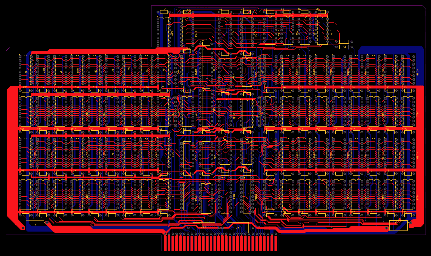
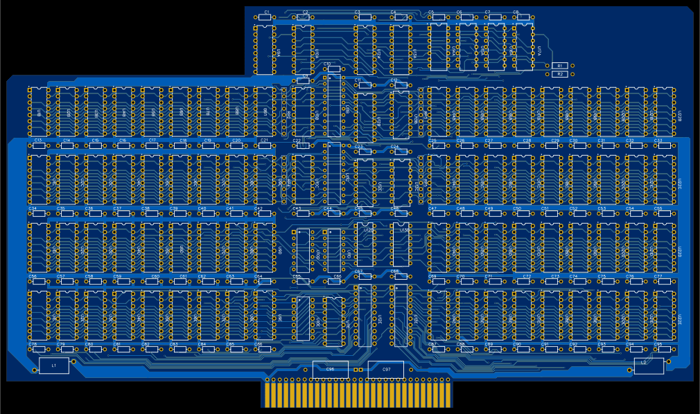
Starting with the RAM card, I pulled everything off of one of mine and got it scanned. The scans need to be redone (I didn't take the levers at the top into account and, as such, the top of the board appears slightly warped in the scans), but the ones I do have are attached here. Once I have better ones, they'll go into a GitHub repository and get posted here. With scans of the front and back of the depopulated board and a set of the schematics in front of me, I got to work. After forty-ish hours and eleventy billion traces later, this is the result:


This is obviously a prototype, and I actually have a question for those out there that know hardware better than I do. The schematics make a distinction between DGND (attached to the ground leads on RAM and RAM bypass caps) and GND (attached to ground on everything else), but the DGND and GND paths are connected. I would have assumed that these would be kept separate, but they're not and I'm not sure why. Anyone able to enlighten me as to why that's the case? Also, the original is a four layer PCB; I've made this as a two layer for now (expanding it to four layer is trivial work, thankfully), but I'm wondering if it genuinely needs the additional two. If you look at the rear scan I attached, you can see that the two RAM sections and the middle logic section are separated on plane three; plane two is completely connected, however. What is the rationale behind this if the grounds are just connected anyway? I'd like to try to keep this a two-layer board if the weird ground planes can be ignored; the cost to manufacture is significantly higher for four layers.
This card still has a bit of work to do before I call it ready to have some produced. I'm having some folks put their eyes on it to make sure there aren't any glaring errors and will upload a set of design files shortly if anyone here wants to take a look as well. Hopefully I can get this thing entirely error free prior to ordering a set, as I really don't want to find myself ordering multiple batches of these, lol. Also, please excuse the component labels, they're just kind of slapped on there at the moment - this thing will look a bit nicer when it's done.
Starting with the RAM card, I pulled everything off of one of mine and got it scanned. The scans need to be redone (I didn't take the levers at the top into account and, as such, the top of the board appears slightly warped in the scans), but the ones I do have are attached here. Once I have better ones, they'll go into a GitHub repository and get posted here. With scans of the front and back of the depopulated board and a set of the schematics in front of me, I got to work. After forty-ish hours and eleventy billion traces later, this is the result:
This is obviously a prototype, and I actually have a question for those out there that know hardware better than I do. The schematics make a distinction between DGND (attached to the ground leads on RAM and RAM bypass caps) and GND (attached to ground on everything else), but the DGND and GND paths are connected. I would have assumed that these would be kept separate, but they're not and I'm not sure why. Anyone able to enlighten me as to why that's the case? Also, the original is a four layer PCB; I've made this as a two layer for now (expanding it to four layer is trivial work, thankfully), but I'm wondering if it genuinely needs the additional two. If you look at the rear scan I attached, you can see that the two RAM sections and the middle logic section are separated on plane three; plane two is completely connected, however. What is the rationale behind this if the grounds are just connected anyway? I'd like to try to keep this a two-layer board if the weird ground planes can be ignored; the cost to manufacture is significantly higher for four layers.
This card still has a bit of work to do before I call it ready to have some produced. I'm having some folks put their eyes on it to make sure there aren't any glaring errors and will upload a set of design files shortly if anyone here wants to take a look as well. Hopefully I can get this thing entirely error free prior to ordering a set, as I really don't want to find myself ordering multiple batches of these, lol. Also, please excuse the component labels, they're just kind of slapped on there at the moment - this thing will look a bit nicer when it's done.
