SE/30 Reloaded - Complete!

craig

Tinkerer
Oct 17, 2021
14
37
13
Dalry, Scotland
www.meerkats.uk.com
Hi all,

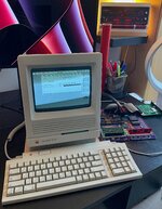
I just wanted to share a few photos of my completed SE/30 rebuild which is now working perfectly thanks to Bolle and a number of others in the vintage Macintosh community. Now I just need to figure out what to use it for! đŸ˜…

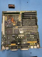
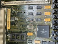
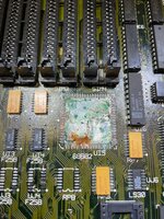
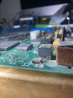
I've included a photo of the original board which was very badly battery-bombed. I did start repairs on it and probably repaired 50% of the broken traces and vias (that I knew about...) before I decided it was a lost cause. Even if I had been successful in getting it "working", it was very unlikely to ever be reliable again due to partially corroded vias. I had previous experience of a less badly bombed SE/30 and although I did get it working again, except for an annoying problem with the serial ports, it took a lot of work!

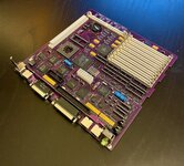
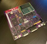
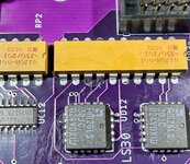
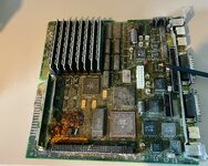
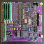
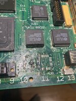
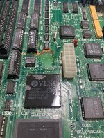
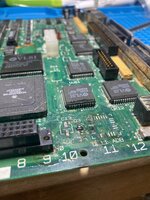
Anyway, without further ado, here are the pics including one of a minor PCB trace fix required on the Rev02 board to swap two serial signal wires over. This is fixed in Rev03 onwards.

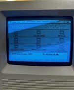
Since I took the photos I have fitted 128MB of RAM but this will be split between two machines once I get the second one built. I expect 64MB is more than enough for anything other than showing off the full 128MB! Snooper also went on to run nearly 300 cycles without any sub-system failures so looking pretty good. I'd love to get a grayscale card fitted so will be watching that project very closely. I also have an ethernet card which I need to test out as it was damaged a bit by the original battery leakage.

Anyway, I hope this helps to inspire anyone thinking of taking on a refurb and please feel free to ask any questions.

Craig.

ps. Mods, I couldn't decide if this post belonged in this forum or the hardware forum so please feel free to move it if I chose wrongly.
 

Attachments

  • bombed.jpeg
    bombed.jpeg
    2.7 MB · Views: 416
  • booted.jpeg
    booted.jpeg
    1.6 MB · Views: 424
  • Finished1.jpeg
    Finished1.jpeg
    1.5 MB · Views: 433
  • Finished5.jpeg
    Finished5.jpeg
    1.7 MB · Views: 462
  • Finished6.jpeg
    Finished6.jpeg
    1.6 MB · Views: 411
  • Finished7.jpeg
    Finished7.jpeg
    1.6 MB · Views: 400
  • PrinterPortFix.jpeg
    PrinterPortFix.jpeg
    1,008 KB · Views: 396

Kai Robinson

TinkerDifferent Board President 2023
Staff member
Founder
Sep 2, 2021
1,102
1
1,122
113
42
Worthing, UK
I'm glad you managed to get a board, after I completely failed to send you one! đŸ˜­
 

craig

Tinkerer
Oct 17, 2021
14
37
13
Dalry, Scotland
www.meerkats.uk.com
I'm glad you managed to get a board, after I completely failed to send you one! đŸ˜­
Haha, don't worry about it Kai, I know you had a lot on your plate with work and then covid. I hope you are feeling much better now and rest assured it was your kind offer of assistance which inspired me to "reload" my SE/30! Getting boards is surprisingly easy given the excellent work from Bolle and the excellent service from JLCPCB.
 

Mu0n

Active Tinkerer
Oct 29, 2021
599
553
93
Quebec
www.youtube.com
Congrats! A worthy effort for a worthy machine.

I'm curious about the amount of time you spent on the repairs of the old board before you decided to switch to a new one?
 

craig

Tinkerer
Oct 17, 2021
14
37
13
Dalry, Scotland
www.meerkats.uk.com
Congrats! A worthy effort for a worthy machine.

I'm curious about the amount of time you spent on the repairs of the old board before you decided to switch to a new one?
Hi, thanks - it is indeed a machine worth saving!

I didn't track time spent on repairing the old board but it was certainly many many hours. If I had to guess I'd say 20+

My strategy was initially to clean the board thoroughly to arrest any ongoing corrosion and then do some visual inspection to identify and repair any simple trace breaks in the bombed area. I also removed my FPU chip to clean underneath it since it was only held on by two remaining solder joints. At this stage I should really have abandoned the board because there was so much visible damage and that is like the proverbial tip of the iceberg compared to what damage you can't see on a 6 layer PCB... However, I still had a sense of optimism having managed to repair a previous battery bombed board albeit one that was less badly damaged.

After fixing visible issues I started doing continuity checks between ROM SIMM data lines and the CPU and PDS sockets. This was an area that needed repair in my previous SE/30 board so I knew which lines to look out for. Sure enough there was similar damage. I then moved on to the address bus and this is where things went south fast! Initially I was just working my way from A0 to A32 but after fixing half a dozen lines I decided to buzz out the entire bus using the address bus connection matrix in the remastered schematics. This is what triggered the decision to abandon the board...

What I found was that for each address line there were anything from 1 to 3 (maybe 4) broken links and almost all of the address lines had at least one break somewhere. This added up to over 40 individual breaks that needed fixing. So for example, perhaps a given address line goes to ROM SIMM, PDS socket, CPU, FPU, Sound chip, SCSI chip, video ROM and various buffer ICs. Typically I would find a break between ROM SIMM and the F258 chips and then maybe another break from there to the PDS slot and maybe another break between there and the CPU and maybe another between the CPU and the sound/scsi/swim/SCC chip. And bear in mind this was after 20+ hours of adding something like 30 bodge wires.

Like I said, I should have abandoned it much earlier or never started in the first place! If I had known then how relatively easy, and infinitely more satisfying, it is to order boards from JLCPCB then I would have taken that route right from the start.

Below are another couple of pics showing the FPU and surrounding area. When I started to clean under the FPU, probably a dozen pads became detached or were already entirely dissolved. Also I have included a pic of the board I WAS able to fix in the state it arrived in. Note how the damage is much more localised towards the corner where the ROMM SIMM meets the PDS socket? Still pretty ugly but as it turns out, much more salvageable.

HTH
 

Attachments

  • IMG_6031.jpeg
    IMG_6031.jpeg
    2.2 MB · Views: 131
  • IMG_6036.jpeg
    IMG_6036.jpeg
    2.4 MB · Views: 159
  • previous_board.jpeg
    previous_board.jpeg
    1.3 MB · Views: 132
  • Like
Reactions: Mu0n

AndyDiags

Tinkerer
Dec 18, 2021
92
161
33
Great job! How many of the original components and ports did you end up not being able to reuse? I see the ram ports are different, but what about the rom and expansion slot, are those new as well? Did it work on your first boot?
 

craig

Tinkerer
Oct 17, 2021
14
37
13
Dalry, Scotland
www.meerkats.uk.com
Great job! How many of the original components and ports did you end up not being able to reuse? I see the ram ports are different, but what about the rom and expansion slot, are those new as well? Did it work on your first boot?

It wasn't so much that I couldn't reuse some of the components and ports, instead I was quite keen to renew as many components as possible, especially parts that were cheap and readily sourced.

So starting with ports, I think I only reused the 14-pin Molex power/video connector and the 64-pin ROM SIMM because I couldn't source those at the time. I have the Molex connector now but it was backordered from Mouser at the time. The ADB, Serial, DB25, DB19, headphone, PDS and RAM SIMM connectors are all brand new, as are all the turned pin chip sockets I used.

As for other components, I used donor ICs for the following:

- CPU, Glue chip, ASC chip, Sony UB10/11 chips, Serial controller chip, SWIM chip, ADB chip, VIA chips and SCSI chip although I could have replaced the SCSI chip.

- Five video PAL chips, UH7 and the video RAM. These are all socketed though so I might replace them at some point.

- Two 26LS30s but that was mainly to avoid having to make a separate order to Utsource just for these two chips.

- UD1 (F240), UA9 (TL071) and I think there was one value of SMD resistor pack that I couldn't source. I forget which though

- Crystals for Y2 and Y3 but Y1 is new. I might replace these too if I can get new ones, especially for Y3 which is a bit corroded.

- RTC chip was destroyed on my original donor so I had to remove one from an SE I also have. But I'm hoping to find a source for RTCs at some point so I can put it back in the SE, or I might build some RTC from the ATTiny85 microcontroller as discussed elsewhere.

Lastly I used all the donor inductors from the bottom side of the PCB and the two switches S1 and S2. And the metal bracket across the back of the board. I think that's about it.

As for first boot - I'd say a qualified "yes" to that question... ;)

What I did was power up the board with a few unnecessary components installed (eg. one ADB port, serial ports, 26LS30 chips, half the RAM SIMM sockets, PDS connector, DB25/19 connectors, RP2/3/10) and without any socketed chips installed first, just to check for correct voltages on caps and VCC-GND on ICs. I found that the 5V was pretty good but 12V was more like 15V due to not being under any load. I then inserted (IIRC) the video PAL chips and I think that gave me some sort of "jail bar" video output before I inserted the remaining chips without any RAM but with ROM SIMM and RTC and video ROM. At each stage I was checking chip temperatures by hand and also rechecking voltages. I forget at which stage I got a boot chime but that was certainly an encouraging moment.

Eventually I put in 4MB of RAM and got a raster and flashing question mark icon before I hooked up my pre-prepared SCSI2SD and it booted right up!

So, if I had been brave/foolish enough to just connect everything up from the start then it would have booted at first power up. But I would definitely encourage a more stepwise approach.

Below is a photo of the board immediately prior to first proper boot up to let you see exactly what was fitted and what wasn't.
 

Attachments

  • first_boot_state.jpeg
    first_boot_state.jpeg
    1.6 MB · Views: 221

AndyDiags

Tinkerer
Dec 18, 2021
92
161
33
Congratulations! Great to hear you didn’t need to spend lots of time on troubleshooting. If someone starts selling kits with all the available parts already included (only transplant parts missing), I can image this will get more popular. Lots of boards out there with leaked batteries, and as good board become more rare over the years, I think the SE/30 reloaded project will pick up.
 

craig

Tinkerer
Oct 17, 2021
14
37
13
Dalry, Scotland
www.meerkats.uk.com
Congratulations! Great to hear you didn’t need to spend lots of time on troubleshooting. If someone starts selling kits with all the available parts already included (only transplant parts missing), I can image this will get more popular. Lots of boards out there with leaked batteries, and as good board become more rare over the years, I think the SE/30 reloaded project will pick up.

Well, you could argue that any time I might have spent troubleshooting was spent instead taking great care during the recovery of donor parts and soldering the new board together! ;)

Joking aside, although I'm a firm believer in people having a go at things that are somewhat outside their comfort zone, it does take a reasonable level of skill and/or experience to build one of these boards. There are a number of factors which will influence the outcome such as:
  • Electronics skill level and experience
  • Quality of soldering equipment and consumables
  • Whether you have a microscope or other similar equipment available
  • Whether you have a hot air station available
  • Whether your donor board components are all still working were it not for the damaged PCB
I've personally been soldering for around 40 years on and off, both as a hobby and as a job but even with the experience I have, I would not be so confident of success without the equipment I have available. That and a healthy dose of luck quite honestly! đŸ˜…

My advice to anyone who already has the skills, or someone who has patience and is willing to learn and perhaps spend some money on equipment, is to go for it! Even if it doesn't boot up first time and some debug is required, believe me it is much better to debug bad solder joints or faulty chips than to debug bad PCB traces and vias! The community is here to help and we're fortunate to have circuit schematics too.
 
  • Love
Reactions: fehervaria

Kai Robinson

TinkerDifferent Board President 2023
Staff member
Founder
Sep 2, 2021
1,102
1
1,122
113
42
Worthing, UK
I just ordered a batch of 5 boards from JLCPCB in standard Green with ENIG gold finish, with the bottom side components populated to speed things up - worked out at £29 per board including shipping and customs. I may have a spare one or two going i can forward on to people.
 

Mikeosoft

New Tinkerer
Feb 10, 2022
6
5
3
Hi I am new here, and stumbled upon this thread just now and actually it is just what I needed to read. I have 2 SE/30 Macintosh. One is currently being recapped and cleaned, but I purchased a second se/30 which had a better looking crt only to discover the mobo is horribly battery bombed and the prior owner removed the caps and looks like attempted to repair it but gave up and took off some chips for parts. Namely the adb chip (not sure the name) but I remembered hearing about this replacement mobo project on Adrian’s digital basement iirc, and then seeing your post here has given me hope. I am not new to soldering, I have been doing it all my life, but I don’t own a hot air gun or a reflow rework station. Thanks for the pictures and the content. I hope to follow in your footsteps and get another se/30 alive again.
 

Attachments

  • 73F18B66-514A-44D5-9C9D-9EACD130C612.jpeg
    73F18B66-514A-44D5-9C9D-9EACD130C612.jpeg
    2.2 MB · Views: 96
  • BA13F887-F56D-4A5B-BEE9-F03F4C51E5AB.jpeg
    BA13F887-F56D-4A5B-BEE9-F03F4C51E5AB.jpeg
    927.3 KB · Views: 96
  • 0A3CDCD4-D493-4386-98C6-D34C39D1B75B.jpeg
    0A3CDCD4-D493-4386-98C6-D34C39D1B75B.jpeg
    2.2 MB · Views: 91
  • F6C030B8-4A09-4A8F-9745-AAB1E5FC4E88.jpeg
    F6C030B8-4A09-4A8F-9745-AAB1E5FC4E88.jpeg
    1.6 MB · Views: 98
  • EE677F49-0A29-489D-AACC-7AE79C64255D.jpeg
    EE677F49-0A29-489D-AACC-7AE79C64255D.jpeg
    1.1 MB · Views: 92
  • Like
Reactions: craig

Kai Robinson

TinkerDifferent Board President 2023
Staff member
Founder
Sep 2, 2021
1,102
1
1,122
113
42
Worthing, UK
Luckily, the ADB chip that was removed, can be sourced from UTSource! They *are* about $12-14 each though, but they're new old stock.

I'd definitely recommend investing in a hot air station - a Yihua one can be purchased for less than $100 off Amazon, I use one, they're not bad as starter gear :)
 
  • Like
Reactions: Mikeosoft

Mikeosoft

New Tinkerer
Feb 10, 2022
6
5
3
Luckily, the ADB chip that was removed, can be sourced from UTSource! They *are* about $12-14 each though, but they're new old stock.

I'd definitely recommend investing in a hot air station - a Yihua one can be purchased for less than $100 off Amazon, I use one, they're not bad as starter gear :)
Will do and thank you all for the help.
 

craig

Tinkerer
Oct 17, 2021
14
37
13
Dalry, Scotland
www.meerkats.uk.com
@Mikeosoft looking at the area around the ADB chip, it looks to me as if the PCB layers have delaminated a bit, probably due to the previous owner using excess heat when removing the chip. This might cause some issues with the vias between layers so might be worth checking continuity of the vias in this area. See if you can feel ripples or large bubbles in the PCB surface to confirm if it has delaminated.

Good luck.

Edit: Yeah I'm an idiot - I read your post out of context and forgot this is a donor board not one you hope to repair. đŸ¤ª

Edit2: Also, although I do have a hot air station, having recently tried out a Chip Quik SMD removal kit, I would seriously suggest considering the Chip Quik, especially when removing donor parts which cannot be sourced elsewhere. It is expensive stuff but it's basically Indium alloy which is a very expensive metal. However, it melts at a much lower temperature than normal solder, especially old, crusty solder, and makes chip removal really easy. A hot air gun is still handy for the final removal but you can do so at a much safer temperature if you've applied chip quik first.
 
Last edited:
  • Like
Reactions: Mikeosoft

Kai Robinson

TinkerDifferent Board President 2023
Staff member
Founder
Sep 2, 2021
1,102
1
1,122
113
42
Worthing, UK
If you're trying to harvest the GLU, don't worry - Porchy reverse engineered it - you can burn the .jed available to an ATF16V8 instead. I also worked out a discrete logic version using 74LVC125's :)
 
  • Like
Reactions: craig and rikerjoe

Kai Robinson

TinkerDifferent Board President 2023
Staff member
Founder
Sep 2, 2021
1,102
1
1,122
113
42
Worthing, UK
@craig the one you found was the one that Porchy did - i did the initial bits that got 90% the way there, but porchy figured out the mad .OE portion of the HAL that made no sense. The discrete version...i'll actually have to dig out my personal macbook pro, see if the project files are still on it đŸ˜›
 
  • Like
Reactions: Mikeosoft