Upgrading IIsi onboard RAM to 4MB

ZeFrenchToon

New Tinkerer
Dec 31, 2022
12
5
3
42
France
Faster RAM is never a problem, it's addressed at the system clock at the same speed as specified RAM. Under spec/marginal RAM speed is a no go as it's not responsive enough at system clock reliably.
Ok but what if …?
We change the crystal to overclock to 25MHz ? 😅
 

Trash80toG4

Active Tinkerer
Apr 1, 2022
910
260
63
Bermuda Triangle, NC USA
That's probably OK for a PDS Card expansion system, don't recall anything about memory issues with that relatively minor uptick?

Contrary to LEM's Mythology, the IIsi system was never intended to be clocked at anything but 20MHz. Yes it shared many components with the IIci, but the 10MHz NuBus adapter clock required is derived from the 20MHz system clock. You'd be overclocking NuBus cards by the same amount. Likely not a great idea?

Gotta take everything on LEM with a grain or up to a lick block of salt. ;)
 
  • Like
Reactions: ZeFrenchToon

Zane Kaminski

Administrator
Staff member
Founder
Sep 5, 2021
371
608
93
Columbus, Ohio, USA
Now wait a minute here. I fear I have created a monster lol—there is no reason to do this mod! It’s a dumb idea! It makes your IIsi slower!!

At the highest supported resolution and color depth, the motherboard RAM in bank A is almost 3x slower than the bank B RAM. As others have said, it’s best to set your disk cache to 768 kB or something to eat up the rest of the slow motherboard RAM so your apps run from the faster SIMMs in bank B. I replaced the chips on my IIsi just to see if it would work, not because it’s a good idea.

So I firmly do not support the idea of the bank A expander board!! Also you have to hook up the bank A multiplexed address (12 pins), bank A write enable (1 pin), bank A RAS and CAS signals (5 pins), and bank A data bus (32 pins). None of those signals are available on any connectors. The SIMM slots all go to the bank B signals which do not suffice for bank A expansion. It’s just not worth it. A lot of soldering is required and all you get is a bunch of slow RAM.

Also the NuBus adapter card has its own 40 MHz crystal which makes the NuBus clock, so overclocking the IIsi doesn’t affect the NuBus.
 
Last edited:
  • Like
Reactions: Fizzbinn and retr01

Fizzbinn

Tinkerer
Nov 29, 2021
189
183
43
Charlottesville, VA
Now wait a minute here. I fear I have created a monster lol—there is no reason to do this mod! It’s a dumb idea! It makes your IIsi slower!!

At the highest supported resolution and color depth, the motherboard RAM in bank A is almost 3x slower than the bank B RAM. As others have said, it’s best to set your disk cache to 768 kB or something to eat up the rest of the slow motherboard RAM so your apps run from the faster SIMMs in bank B. I replaced the chips on my IIsi just to see if it would work, not because it’s a good idea.

Zane, I agree with you with one caveat, if you are not using built-in video (i.e you are using a PDS or NuBus video card) you *could* make the case that you want more then 65MB of RAM: Bank A 1MB (fixed), Bank B 64MB (4x 16MB SIMMs). I personally don't see the need for this other then the perfectly valid because I can and it would be cool/fun to do rationale :) But if you do intend to use the built-in video then you are accepting a significant system performance drop by using ANY Bank A Ram for running the system and/or programs.

Its not that Bank A RAM is inherently slower than Bank B RAM so much as it is IF you use built-in video Bank A is slowed down for CPU use by time sharing it with the built-in video system.

There is good explanation of the CPU slow down issue with using RAM based built-in video (RBV) on page 25 of the IIsi Hardware Developer Note:

"The RBV and Bank A of DRAM share a separate RAM data bus that can be connected to or disconnected from the CPU data bus by the bus buffers (see “Use of RAM by the Video” in Chapter 3). Data stored in Bank A of system DRAM is used by the RBV to feed a constant stream of video data to the display monitor during the live video portion of each horizontal screen line. The RBV asks the MDU for data as it is needed; the MDU responds by disconnecting the RAM data bus from the CPU data bus and performing an eight-longword DMA (direct-memory access) burst read from RAM while clocking the read data into the RBV FIFO (first in, first out) buffer.​
If a video burst is in progress, a CPU access to RAM Bank A is delayed, effectively slowing down the CPU. This effect is more pronounced for the larger monitors and for more bits per pixel. Note that only accesses to RAM Bank A are affected by video. The optional Bank B of DRAM connects directly to the CPU data bus, and the CPU has full access to this bank at all times, as it does to ROM and the I/O devices."​

Diagram from page 23:

1683166136270.png
 

Trash80toG4

Active Tinkerer
Apr 1, 2022
910
260
63
Bermuda Triangle, NC USA
Yep, Vampire Video slows things down, but it's only enabled if sense line signals are detected on the connector
at startup and the buffering setup kicks in. As in pulling the Video ROM in the SE/30, $E built-in video also disappears from the Slot Manager Report in the IIsi.

Moral of the story, find a way to avoid using onboard video of the IIsi at all costs, it's all but crap anyway. The only truly useful (high) resolution is Portrait amd then at only 4bit.
 

Fizzbinn

Tinkerer
Nov 29, 2021
189
183
43
Charlottesville, VA
Yep, Vampire Video slows things down, but it's only enabled if sense line signals are detected on the connector
at startup and the buffering setup kicks in. As in pulling the Video ROM in the SE/30, $E built-in video also disappears from the Slot Manager Report in the IIsi.

Moral of the story, find a way to avoid using onboard video of the IIsi at all costs, it's all but crap anyway. The only truly useful (high) resolution is Portrait amd then at only 4bit.

Good point that if you don't connect anything to the built-in video that means that the system is not using RAM based built-in video (RBV) so Bank A and B are equally as performant.

it's only "Vampire Video" if you try to use Bank A RAM for System/Program memory and make use of the built-in video. If you use the RAM muncher extension or set the Disk Cache to 768KB you force all System/Program RAM usage to Bank B and the performance penalty is moot. In that situation you can think of RAM Bank A as sort of dedicated video RAM, and it's actually not bad at all video performance wise if 256 colors at 640x480 is all that you are interested in. That is it holds its own against PDS and NuBus Video cards driving a display with 256 colors at 640x480.
 
Last edited:

Trash80toG4

Active Tinkerer
Apr 1, 2022
910
260
63
Bermuda Triangle, NC USA
So I firmly do not support the idea of the bank A expander board!! Also you have to hook up the bank A multiplexed address (12 pins), bank A write enable (1 pin), bank A RAS and CAS signals (5 pins), and bank A data bus (32 pins). None of those signals are available on any connectors. The SIMM slots all go to the bank B signals which do not suffice for bank A expansion. It’s just not worth it. A lot of soldering is required and all you get is a bunch of slow RAM.
Not slow if you're avoiding the Vampire Video anchor. ;)

Best diagram I could come up with quickly from what I've posted on MLA:

Here are the only three(?) lines you need to jumper directly from MDU above in order to address a high capacity 72-pin SIMM fom Bank A of the IIsi. ISTR there maybe being a fourth?

BankA-GAMMA-001.jpg


All other signals connect to the SIMM from the pads of Bank A as I recall. Again, use of a real VidCard with nothing connected to video out of the IIsi is a must.

Also the NuBus adapter card has its own 40 MHz crystal which makes the NuBus clock, so overclocking the IIsi doesn’t affect the NuBus.
We need to hear from @Bolle on this one. The IIsi NuBus Adapter from Radius that "just works" in the SE/30 does so at only 8MHz, halved from the 16MHz system bus there and at 10MHz from the 20MHz system bus of the IIsi.

Though fast, I'm guessing that the 40MHz crystal on the Apple Adapter may be for the asynchronous CoPro? Can you just have a pair of 40MHz crystals running amok in tandem? I didn't think that worked?

_____________________________________________

edit: looking at it, I think it was A9 and A10 that needed to be jumpered from MDU in addition to A11. Out of town ATM, so my archive of lost MLA attachents is back home.
 
Last edited:

Zane Kaminski

Administrator
Staff member
Founder
Sep 5, 2021
371
608
93
Columbus, Ohio, USA
All other signals connect to the SIMM from the pads of Bank A as I recall. Again, use of a real VidCard with nothing connected to video out of the IIsi is a must.
Nope, all the bank A and bank B RAM array pins are totally separate. And it makes sense if you think about it. If the bank A address or data bus were connected to the bank B chips, how could bank A be doing video stuff while bank B is concurrently serving the 68030? All the pins are separate and so you would need to jumper to all 50 pins (32 data, 12 address, 4 CAS, 1 RAS, 1 write enable).

Can you just have a pair of 40MHz crystals running amok in tandem? I didn't think that worked?
The NuChip is designed for asynchronous operation between the 68030 bus and the NuBus. So internally it has two clock domains and carefully passes signals between them to coordinate the timing. The same chip as on the IIsi NuBus adapter is on the IIci motherboard and on there it connects to the 25 MHz 68030 bus clock domain and the 10 MHz NuBus clock domain. So this is why I concluded that the 68030 bus clock is independent of the NuBus clock when it comes to the NuChip bridge.
 

Trash80toG4

Active Tinkerer
Apr 1, 2022
910
260
63
Bermuda Triangle, NC USA
Yep, I know about the two full sets of connections for banks A and B on MDU, but most are available on the Bank A memory pads. It's been at least five years, so I'm thinking RAS2 would need to be jumpered from MDU along with A9 and A10 for six bodge wires in total to support 64MB in a Bank A bodge?

D0-31, A0-8, RAS0 and CAS0-3 lines are all available on the pads in Bank A. If I'm reading that right we need only jumper RAS1-3 and A9-11 to fill the bill?

Dunno, dog tired and eyes aren't tracking together when I try to count this up, sorry. 🤪
 
Last edited:

Trash80toG4

Active Tinkerer
Apr 1, 2022
910
260
63
Bermuda Triangle, NC USA
The same chip as on the IIsi NuBus adapter is on the IIci motherboard and on there it connects to the 25 MHz 68030 bus clock domain and the 10 MHz NuBus clock domain. So this is why I concluded that the 68030 bus clock is independent of the NuBus clock when it comes to the NuChip bridge.
Makes sense, in the DuoDock you have the same 25MHz system bus, NuChip and a 40MHz crystal. Maybe it's only the Radius NuBus adapter that's dependent upon system clock for timing? Curiouser and curiouser. :oops:
 

Zane Kaminski

Administrator
Staff member
Founder
Sep 5, 2021
371
608
93
Columbus, Ohio, USA
Yep, I know about the two full sets of connections for banks A and B on MDU, but most are available on the Bank A memory pads. It's been at least five years, so I'm thinking RAS2 would need to be jumpered from MDU along with A9 and A10 for six bodge wires in total to support 64MB in a Bank A bodge?

D0-31, A0-8, RAS0 and CAS0-3 lines are all available on the pads in Bank A. If I'm reading that right we need only jumper RAS1-3 and A9-11 to fill the bill?

Dunno, dog tired and eyes aren't tracking together when I try to count this up, sorry. 🤪
Maybe we’re confusing bank A and B. When I say bank A I mean the soldered RAM used for video. Bank B is the SIMM slots. So yeah, you can get all those signals on the pads of the bank A chips, but it’s like 50 things you need to connect to. Is that what you mean?
 

Trash80toG4

Active Tinkerer
Apr 1, 2022
910
260
63
Bermuda Triangle, NC USA
Yep! Banks A & B are defined in the docs, A is the buffered Vampire Video kluge.

There are quite a few, but much less adventurous IC to SIMM conversions in terms of pin count out there. Gotta get the SuperIIsi build up to match the SE/30 spec. Don't really need to though. Rocket33 will power it, so more of a street cred thing if I can pull it off. PowerCache P33 is the alternate config, for that the extra 63MB is a necessity. ;)
 

Zane Kaminski

Administrator
Staff member
Founder
Sep 5, 2021
371
608
93
Columbus, Ohio, USA
@Trash80toG4 tbh I don’t really understand the purpose. It’s quite a lot of work to do the mod you’re proposing. Maybe we should just make an accelerator for the IIsi with 128 MB onboard RAM lol. 40 MHz sounds good enough as long as it’s paired with a fast burstable RAM system and some L2 cache. Maybe once I finish the WarpSE
 
  • Love
  • Like
Reactions: JeffC and retr01

Trash80toG4

Active Tinkerer
Apr 1, 2022
910
260
63
Bermuda Triangle, NC USA
@Trash80toG4 tbh I don’t really understand the purpose. It’s quite a lot of work to do the mod you’re proposing.
It's a crazy project from many years ago, an offshoot of the SuperIIsi-AKA-SE/30's bane project. Was curious to see what you had to say about the concept of a 128MB hack for the IIsi.

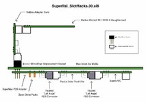
A new accelerator seems like a good idea for the somewhen, but NOBODY was doing anything like that back then. SuperIIsi is a Radius Rocket 33/128MB powered hack with the PDS slot broken out the bottom with VidCard and NIC running across the underside of the MoBo. In that config, crappy vampire video running 4bit portrait GS makes a fine secondary screen, no system performance hit. Too bad I can only get the Rocket up and running under RocketShare

SuperIIsi_SlotHacks.30.2p.jpg

Didn't know termination resistor packs were the order of the day, I'd thought the empty pads might have been for zeners to quiet things down.

Sorry to take this so far afield, LOVE your 4MB Bank A hack. Shades of doing same for 512k in the 128k back in the day,
 

JeffC

Tinkerer
Sep 26, 2021
122
79
28
Seattle, WA
That's probably OK for a PDS Card expansion system, don't recall anything about memory issues with that relatively minor uptick?

Contrary to LEM's Mythology, the IIsi system was never intended to be clocked at anything but 20MHz. Yes it shared many components with the IIci, but the 10MHz NuBus adapter clock required is derived from the 20MHz system clock. You'd be overclocking NuBus cards by the same amount. Likely not a great idea?

Gotta take everything on LEM with a grain or up to a lick block of salt. ;)

Does overclocking to 25mhz cause a problem with NuBus video cards using a PDS -> NuBus adapter?
 

Trash80toG4

Active Tinkerer
Apr 1, 2022
910
260
63
Bermuda Triangle, NC USA
Apparently not. I started a thread over yonder asking about just that, but nobody reported any experiences. Was wondering about that given the results @Bolle reported in testing the Radius NuBus Adapter that @joethezombie found when we were working on the SE/30 PowerCache Adapter project.

I'm happy @Zane Kaminski corrected me as I'd conflated the Radius setup with Apple's. As I said, this was years ago and I'm delighted to learn that NuChip is asynchronous. Should have realized that from my study of the DuoDock's NuBus setup. I'm back to adapting that one to the SE/30 as the next step in the quest for NuBus in SE/30.
 
  • Like
Reactions: JeffC

Trash80toG4

Active Tinkerer
Apr 1, 2022
910
260
63
Bermuda Triangle, NC USA
Maybe we should just make an accelerator for the IIsi with 128 MB onboard RAM lol. 40 MHz sounds good enough as long as it’s paired with a fast burstable RAM system and some L2 cache. Maybe once I finish the WarpSE
That's a great idea, it's really growing on me, most especially if it's designed to work directly off the PDS in the bottom of a TwinSlot adapter in the IIsi and so would have a passthru/form factor to be at the bottom of a stack of cards in the SE/30. ;)

Neat stuff on form factors in his thread:

edit: I think you should start an exploratory thread for that project. I need some Illustrator time to do form factor studies. :)
 
Last edited:

Trash80toG4

Active Tinkerer
Apr 1, 2022
910
260
63
Bermuda Triangle, NC USA
Maybe we should just make an accelerator for the IIsi with 128 MB onboard RAM lol. 40 MHz sounds good enough as long as it’s paired with a fast burstable RAM system and some L2 cache. Maybe once I finish the WarpSE
That's a great idea, really growing on me, most especially if it's designed to work directly off the PDS in the bottom of a TwinSlot adapter and has a passthru/form factor to be the bottom of a stack of cards in the SE/30. ;)
 

retr01

Senior Tinkerer
Jun 6, 2022
2,473
1
793
113
Utah, USA
retr01.com
Modern accelerators may be flexible enough to offer other things on the same board besides more RAM that may eventually negate the need for risers like the TwinSpark.

WiFi chips are small, so a chipset can emulate 10/100 networking, while a graphics chipset can emulate graphic cards.