Hi everyone.
I wanted to post about my new design for a 25 MHz 68HC000-based Macintosh SE accelerator. As usual with my gizmos, this is a collaboration with Garrett Fellers of Garrett's Workshop. I'm the principal designer and Garrett is the codesigner and he manufactures our boards.
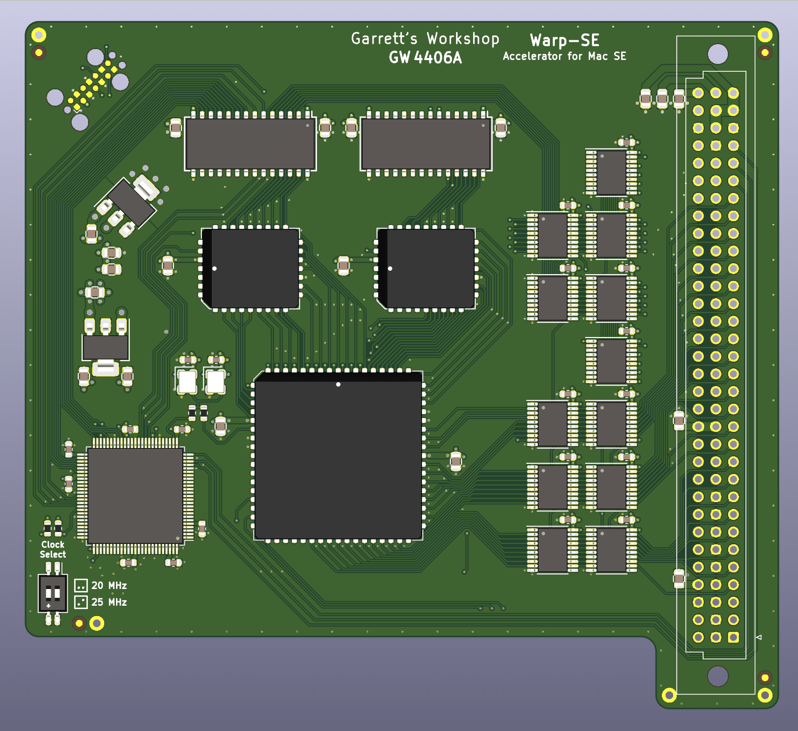
My aim with this card is to achieve a speedup of 3x or so while maintaining the greatest degree of compatibility with applications. Therefore I have employed an MC68HC000 running at up to 25 MHz instead of an '030. The card has 4 MB of legacy 60ns DRAM onboard which can be accessed with 0 wait states at 25 MHz. The Macintosh SE ROM is also reproduced on the board in two 512kx8 70ns flash ROMs. In order to achieve the requisite 3x speedup on graphics performance, I have implemented a longword posted write buffer. This lets the accelerated CPU write to video/sound memory up to twice in a row with 0 wait states. The accelerator trickles out these writes from the fast CPU to the slower PDS bus while the fast CPU gets to continue executing from RAM or ROM memory on the card. CPU speed is selectable, either 20 MHz or 25 MHz. The current board is using the Xilinx XC95144XL-10TQG100C CPLD to implement the control logic but that's just because we at GW have a few trays of them from a cancelled project. The control logic is amenable to implementation in the Lattice LC4128Z/E/C/B/V CPLD too.
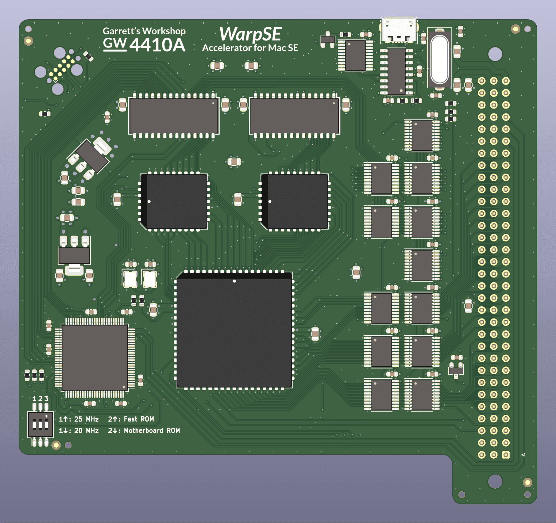
The CPLD on the bottom left controls everything. Here's a block diagram of the system including several functional units inside the CPLD as well as external components like the ROM, RAM, 68k CPU, and the latches for the posted write buffer.
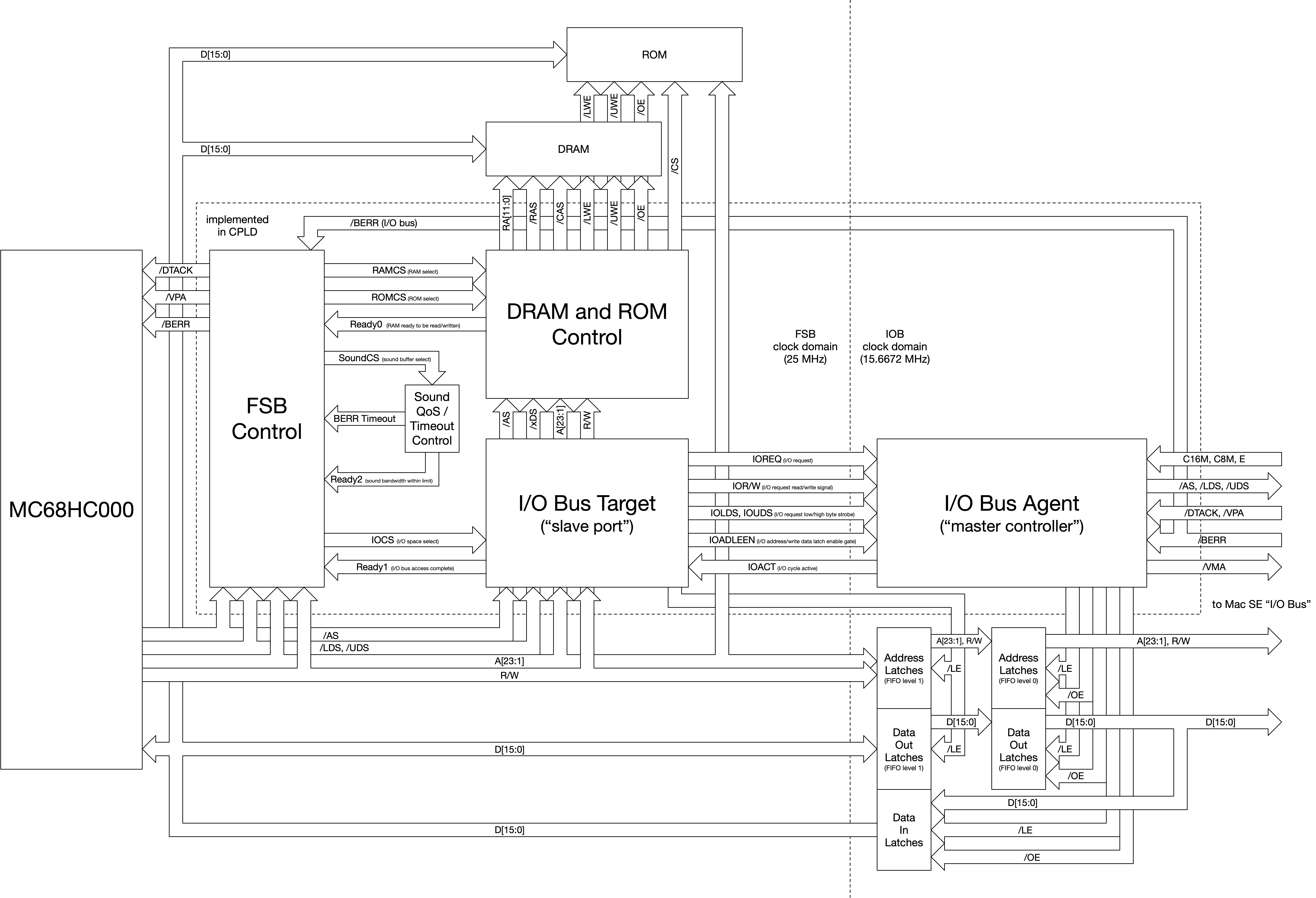
Of course, my description above sort of just scratches the surface. There are four main blocks in the CPLD shown in the diagram above. These are the FSB controller, DRAM/ROM controller, I/O bus target (i.e. slave port), and I/O bus agent (i.e. master controller). I have tried my best to specify the behavior of these blocks in my timing diagrams available here: https://garrettsworkshop.github.io/WarpSE/Documentation/index.html
These are complicated but I'm hoping some of our skilled members can take a look. The diagrams are a bit of a work in progress but I believe they all basically make sense.
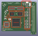
Here's an annotated render of the board showing where the external components are placed:
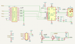
One interesting feature that I have added partway through development is the USB update system. I am using the inexpensive CH340G USB-to-serial chip to bit-bang the CPLD's JTAG port in order to do a software update. The data rate is pretty slow, maximum 1 kbit/sec, so it will take several minutes to update the CPLD. Nevertheless it's totally worth it since the additional cost for the update system is quite low. Here's the schematic for the update part of the system:
Source: https://github.com/garrettsworkshop/Warp-SE
I am of course looking for feedback, but my main aim in posting this documentation is to get some information out there on how to design an accelerator. Boards and PAL/GAL images are good to reverse engineer for study and reproduction, but with that approach you don't get get to hear from the designer about the tradeoffs and reasoning. I think my design methodology works well and I will teach it to anyone who's interested and has the required prerequisite knowledge. I like designing by myself and with Garrett but we are feeling lonely! It would be good to get some collaborative projects going where the understanding of how they work is distributed among the community rather than just with a few people. So this big dump of documentation is my attempt to start down that path.
FAQ - Here are some questions which others have asked me privately and figured I'd post a condensed version of their question and my answer.
Q: What is the "sound QoS" or "sound rate limiter?"
A: It's a fix for a behavior in the sound driver in the Mac ROM that causes audio glitches when running with an accelerated processor. The sound driver regenerates the samples in the sound buffer following vblank. Generating the sound samples takes a while and the sound driver has to be careful that it doesn't write into the buffer such that that samples yet to be played are overwritten. Therefore the sound driver starts updating the buffer at a different index depending on the sound generation mode. Modes that generate samples quickly have to start further away from the current sample being played so that they don't cross over the current playback index, causing glitches in the sound output. In four-voice mode, the samples take longer to generate, so the sound driver begins updating samples closer to the current index being played. With an accelerated CPU, the samples are generated faster and so the current sample being played is overwritten. The fix for this is to slow the CPU way down when accessing the sound buffer.
Q: What are "test vectors?"
A: Test vectors are waveform sequences used to verify that a digital system is working as expected. They're like test cases in software development. The methodology goes like this... We make test vectors which correspond to the behavior of the system surrounding a system under test. So in this case the system under test is the accelerator control logic and the test vectors should represent expected behaviors of the BBU, MC68HC000, etc. All of the timing diagrams in the documentation on GitHub are good candidates to turn into test vectors. These are combined with the compiled system control logic and simulated so we can see how the control logic will behave when installed in the Mac (as long as our test vectors represent the actual behavior of the system). Generally there are also output vectors that show the expected behavior of the system under test too, and any deviation from the expected output vectors is flagged as a failed test case.
Project Status
Accelerator is working in the lab, with a reported 3.25x overall speedup in Speedometer 3.
To-Do Board
I wanted to post about my new design for a 25 MHz 68HC000-based Macintosh SE accelerator. As usual with my gizmos, this is a collaboration with Garrett Fellers of Garrett's Workshop. I'm the principal designer and Garrett is the codesigner and he manufactures our boards.
My aim with this card is to achieve a speedup of 3x or so while maintaining the greatest degree of compatibility with applications. Therefore I have employed an MC68HC000 running at up to 25 MHz instead of an '030. The card has 4 MB of legacy 60ns DRAM onboard which can be accessed with 0 wait states at 25 MHz. The Macintosh SE ROM is also reproduced on the board in two 512kx8 70ns flash ROMs. In order to achieve the requisite 3x speedup on graphics performance, I have implemented a longword posted write buffer. This lets the accelerated CPU write to video/sound memory up to twice in a row with 0 wait states. The accelerator trickles out these writes from the fast CPU to the slower PDS bus while the fast CPU gets to continue executing from RAM or ROM memory on the card. CPU speed is selectable, either 20 MHz or 25 MHz. The current board is using the Xilinx XC95144XL-10TQG100C CPLD to implement the control logic but that's just because we at GW have a few trays of them from a cancelled project. The control logic is amenable to implementation in the Lattice LC4128Z/E/C/B/V CPLD too.
The CPLD on the bottom left controls everything. Here's a block diagram of the system including several functional units inside the CPLD as well as external components like the ROM, RAM, 68k CPU, and the latches for the posted write buffer.
Of course, my description above sort of just scratches the surface. There are four main blocks in the CPLD shown in the diagram above. These are the FSB controller, DRAM/ROM controller, I/O bus target (i.e. slave port), and I/O bus agent (i.e. master controller). I have tried my best to specify the behavior of these blocks in my timing diagrams available here: https://garrettsworkshop.github.io/WarpSE/Documentation/index.html
These are complicated but I'm hoping some of our skilled members can take a look. The diagrams are a bit of a work in progress but I believe they all basically make sense.
Here's an annotated render of the board showing where the external components are placed:

One interesting feature that I have added partway through development is the USB update system. I am using the inexpensive CH340G USB-to-serial chip to bit-bang the CPLD's JTAG port in order to do a software update. The data rate is pretty slow, maximum 1 kbit/sec, so it will take several minutes to update the CPLD. Nevertheless it's totally worth it since the additional cost for the update system is quite low. Here's the schematic for the update part of the system:

Source: https://github.com/garrettsworkshop/Warp-SE
I am of course looking for feedback, but my main aim in posting this documentation is to get some information out there on how to design an accelerator. Boards and PAL/GAL images are good to reverse engineer for study and reproduction, but with that approach you don't get get to hear from the designer about the tradeoffs and reasoning. I think my design methodology works well and I will teach it to anyone who's interested and has the required prerequisite knowledge. I like designing by myself and with Garrett but we are feeling lonely! It would be good to get some collaborative projects going where the understanding of how they work is distributed among the community rather than just with a few people. So this big dump of documentation is my attempt to start down that path.
FAQ - Here are some questions which others have asked me privately and figured I'd post a condensed version of their question and my answer.
Q: What is the "sound QoS" or "sound rate limiter?"
A: It's a fix for a behavior in the sound driver in the Mac ROM that causes audio glitches when running with an accelerated processor. The sound driver regenerates the samples in the sound buffer following vblank. Generating the sound samples takes a while and the sound driver has to be careful that it doesn't write into the buffer such that that samples yet to be played are overwritten. Therefore the sound driver starts updating the buffer at a different index depending on the sound generation mode. Modes that generate samples quickly have to start further away from the current sample being played so that they don't cross over the current playback index, causing glitches in the sound output. In four-voice mode, the samples take longer to generate, so the sound driver begins updating samples closer to the current index being played. With an accelerated CPU, the samples are generated faster and so the current sample being played is overwritten. The fix for this is to slow the CPU way down when accessing the sound buffer.
Q: What are "test vectors?"
A: Test vectors are waveform sequences used to verify that a digital system is working as expected. They're like test cases in software development. The methodology goes like this... We make test vectors which correspond to the behavior of the system surrounding a system under test. So in this case the system under test is the accelerator control logic and the test vectors should represent expected behaviors of the BBU, MC68HC000, etc. All of the timing diagrams in the documentation on GitHub are good candidates to turn into test vectors. These are combined with the compiled system control logic and simulated so we can see how the control logic will behave when installed in the Mac (as long as our test vectors represent the actual behavior of the system). Generally there are also output vectors that show the expected behavior of the system under test too, and any deviation from the expected output vectors is flagged as a failed test case.
Project Status
Accelerator is working in the lab, with a reported 3.25x overall speedup in Speedometer 3.
To-Do Board
| Frozen | All but done | Needs work | Not yet started |
|---|---|---|---|
| Parts selection: CPLD, RAM, ROM | CPLD verilog | ||
| Schematic | Documentation & timing diagrams | ||
| Board layout | Prototype board bringup |
Hi everyone.
I wanted to post about my new design for a 25 MHz 68HC000-based Macintosh SE accelerator. As usual with my gizmos, this is a collaboration with Garrett Fellers of Garrett's Workshop. I'm the principal designer and Garrett is the codesigner and he manufactures our boards.
My aim with this card is to achieve a speedup of 3x or so while maintaining the greatest degree of compatibility with applications. Therefore I have employed an MC68HC000 running at up to 25 MHz instead of an '030. The card has 4 MB of legacy 60ns DRAM onboard which can be accessed with 0 wait states at 25 MHz. The Macintosh SE ROM is also reproduced on the board in two 512kx8 70ns flash ROMs. In order to achieve the requisite 3x speedup on graphics performance, I have implemented a longword posted write buffer (hence the multitude of '573 latches near the PDS connector). This lets the accelerated CPU write to video/sound memory up to twice in a row with 0 wait states. The accelerator trickles out these writes from the fast CPU to the slower PDS bus while the fast CPU gets to continue executing from RAM or ROM memory on the card. CPU speed is selectable, either 20 MHz or 25 MHz. The current board is using the Xilinx XC95144XL-10TQG100C CPLD to implement the control logic but that's just because we at GW have a few trays of them from a cancelled project. The control logic is amenable to implementation in the Lattice LC4128Z/E/C/B/V CPLD too.
Source is available here: https://github.com/garrettsworkshop/Warp-SE
The CPLD on the bottom left controls everything. Here's a block diagram of the system including the several blocks inside the CPLD (zooming in required lol):

Of course, my description above sort of just scratches the surface. There are four main blocks in the CPLD shown in the diagram above. These are the FSB controller, DRAM/ROM controller, I/O bus target (i.e. slave port), and I/O bus agent (i.e. master controller). I have tried my best to specify the behavior of these blocks in my timing diagrams available here: https://garrettsworkshop.github.io/Warp-SE/Docs/index.html
These are complicated but I'm hoping some of our skilled members can take a look. The diagrams are a bit of a work in progress but I believe diagrams 0 through 16 are correct. Diagrams 17 through 26 are half done. Every timing diagram (but for a few at the end which I haven't finished) has a detailed explanation of what's going on and why.
I am of course looking for feedback, but my main aim in posting this documentation is to get some information out there on how to design an accelerator. Boards and PAL/GAL images are good to reverse engineer for study and reproduction, but with that approach you don't get get to hear from the designer about the tradeoffs and reasoning. I think my design methodology works well and I will teach it to anyone who's interested and has the required prerequisite knowledge. I like designing by myself and with Garrett but we are feeling lonely! It would be good to get some collaborative projects going where the understanding of how they work is distributed among the community rather than just with a few people. So this big dump of documentation is my attempt to start down that path.
Expect updates to the timing diagrams! I have yet to finish diagrams 17-20 and diagrams 21-26 are missing the explanation. I'll get to that in the next day or so. I welcome all questions no matter how simple but hopefully we can keep the conversation here regarding engineering rather than organizational questions like when the board will be available, etc.
FAQ - Here are some questions which others have asked me privately and figured I'd post a condensed version of their question and my answer.
Q: What is the "sound QoS" or "sound rate limiter?"
A: It's a fix for a behavior in the sound driver in the Mac ROM that causes audio glitches when running with an accelerated processor. The sound driver regenerates the samples in the sound buffer following vblank. Generating the sound samples takes a while and the sound driver has to be careful that it doesn't write into the buffer such that that samples yet to be played are overwritten. Therefore the sound driver starts updating the buffer at a different index depending on the sound generation mode. Modes that generate samples quickly have to start further away from the current sample being played so that they don't cross over the current playback index, causing glitches in the sound output. In four-voice mode, the samples take longer to generate, so the sound driver begins updating samples closer to the current index being played. With an accelerated CPU, the samples are generated faster and so the current sample being played is overwritten. The fix for this is to slow the CPU way down when accessing the sound buffer.
Q: What are "test vectors?"
A: Test vectors are waveform sequences used to verify that a digital system is working as expected. They're like test cases in software development. The methodology goes like this... We make test vectors which correspond to the behavior of the system surrounding a system under test. So in this case the system under test is the accelerator control logic and the test vectors should represent expected behaviors of the BBU, MC68HC000, etc. All of the timing diagrams in the documentation on GitHub are good candidates to turn into test vectors. These are combined with the compiled system control logic and simulated so we can see how the control logic will behave when installed in the Mac (as long as our test vectors represent the actual behavior of the system). Generally there are also output vectors that show the expected behavior of the system under test too, and any deviation from the expected output vectors is flagged as a failed test case.
Project Status/To-Do
Here's my attempt to keep track of the project to-do. Stuff in the "frozen" category is assumed not to be changing for the currently-planned release. "All but done" is stuff close to being finished or able to commit to but maybe we need to do some more simulation or something. "Needs work," is stuff that... needs work.
I wanted to post about my new design for a 25 MHz 68HC000-based Macintosh SE accelerator. As usual with my gizmos, this is a collaboration with Garrett Fellers of Garrett's Workshop. I'm the principal designer and Garrett is the codesigner and he manufactures our boards.
My aim with this card is to achieve a speedup of 3x or so while maintaining the greatest degree of compatibility with applications. Therefore I have employed an MC68HC000 running at up to 25 MHz instead of an '030. The card has 4 MB of legacy 60ns DRAM onboard which can be accessed with 0 wait states at 25 MHz. The Macintosh SE ROM is also reproduced on the board in two 512kx8 70ns flash ROMs. In order to achieve the requisite 3x speedup on graphics performance, I have implemented a longword posted write buffer (hence the multitude of '573 latches near the PDS connector). This lets the accelerated CPU write to video/sound memory up to twice in a row with 0 wait states. The accelerator trickles out these writes from the fast CPU to the slower PDS bus while the fast CPU gets to continue executing from RAM or ROM memory on the card. CPU speed is selectable, either 20 MHz or 25 MHz. The current board is using the Xilinx XC95144XL-10TQG100C CPLD to implement the control logic but that's just because we at GW have a few trays of them from a cancelled project. The control logic is amenable to implementation in the Lattice LC4128Z/E/C/B/V CPLD too.
Source is available here: https://github.com/garrettsworkshop/Warp-SE
The CPLD on the bottom left controls everything. Here's a block diagram of the system including the several blocks inside the CPLD (zooming in required lol):
Of course, my description above sort of just scratches the surface. There are four main blocks in the CPLD shown in the diagram above. These are the FSB controller, DRAM/ROM controller, I/O bus target (i.e. slave port), and I/O bus agent (i.e. master controller). I have tried my best to specify the behavior of these blocks in my timing diagrams available here: https://garrettsworkshop.github.io/Warp-SE/Docs/index.html
These are complicated but I'm hoping some of our skilled members can take a look. The diagrams are a bit of a work in progress but I believe diagrams 0 through 16 are correct. Diagrams 17 through 26 are half done. Every timing diagram (but for a few at the end which I haven't finished) has a detailed explanation of what's going on and why.
I am of course looking for feedback, but my main aim in posting this documentation is to get some information out there on how to design an accelerator. Boards and PAL/GAL images are good to reverse engineer for study and reproduction, but with that approach you don't get get to hear from the designer about the tradeoffs and reasoning. I think my design methodology works well and I will teach it to anyone who's interested and has the required prerequisite knowledge. I like designing by myself and with Garrett but we are feeling lonely! It would be good to get some collaborative projects going where the understanding of how they work is distributed among the community rather than just with a few people. So this big dump of documentation is my attempt to start down that path.
Expect updates to the timing diagrams! I have yet to finish diagrams 17-20 and diagrams 21-26 are missing the explanation. I'll get to that in the next day or so. I welcome all questions no matter how simple but hopefully we can keep the conversation here regarding engineering rather than organizational questions like when the board will be available, etc.
FAQ - Here are some questions which others have asked me privately and figured I'd post a condensed version of their question and my answer.
Q: What is the "sound QoS" or "sound rate limiter?"
A: It's a fix for a behavior in the sound driver in the Mac ROM that causes audio glitches when running with an accelerated processor. The sound driver regenerates the samples in the sound buffer following vblank. Generating the sound samples takes a while and the sound driver has to be careful that it doesn't write into the buffer such that that samples yet to be played are overwritten. Therefore the sound driver starts updating the buffer at a different index depending on the sound generation mode. Modes that generate samples quickly have to start further away from the current sample being played so that they don't cross over the current playback index, causing glitches in the sound output. In four-voice mode, the samples take longer to generate, so the sound driver begins updating samples closer to the current index being played. With an accelerated CPU, the samples are generated faster and so the current sample being played is overwritten. The fix for this is to slow the CPU way down when accessing the sound buffer.
Q: What are "test vectors?"
A: Test vectors are waveform sequences used to verify that a digital system is working as expected. They're like test cases in software development. The methodology goes like this... We make test vectors which correspond to the behavior of the system surrounding a system under test. So in this case the system under test is the accelerator control logic and the test vectors should represent expected behaviors of the BBU, MC68HC000, etc. All of the timing diagrams in the documentation on GitHub are good candidates to turn into test vectors. These are combined with the compiled system control logic and simulated so we can see how the control logic will behave when installed in the Mac (as long as our test vectors represent the actual behavior of the system). Generally there are also output vectors that show the expected behavior of the system under test too, and any deviation from the expected output vectors is flagged as a failed test case.
Project Status/To-Do
Here's my attempt to keep track of the project to-do. Stuff in the "frozen" category is assumed not to be changing for the currently-planned release. "All but done" is stuff close to being finished or able to commit to but maybe we need to do some more simulation or something. "Needs work," is stuff that... needs work.
| Frozen | All but done | Needs work |
| Parts selection: CPLD, RAM, ROM | Board layout | Test vectors (copy these from documentation) |
| Schematic | CPLD verilog | |
| Documentation & timing diagrams |
Last edited:

