Radius FPD/SE - Rotation Transform/HDMI Output via FPGA Project Board - CLAUDE SESSIONS

Trash80toG4

Active Tinkerer
Apr 1, 2022
1,481
480
83
Bermuda Triangle, NC USA
Good eye — that continuous line is real. Zooming into just the photo (no overlay), you can see the trace itself runs right through the ink stamp without interruption — the ink is sitting on top of the solder mask, so seeing copper trace geometry "through" it just confirms it's genuinely part of the board surface at that spot, not a stamp artifact.

But before jumping to a 4-layer buried-plane explanation, I'd want to rule out a much simpler one: U25 and U26 are unimplemented footprints — nothing ever gets soldered there. If Radius's layout software saw those two pad rings as dead space (no populated pins to keep clear of), running an ordinary 2-layer trace straight through the middle of that footprint costs nothing and avoids needing a jog around it. That would fully explain a trace visually "connecting" U25 and U26 without needing anything exotic — it's not really connecting the footprints at all, just happening to physically transit the space between their pads on its way somewhere else on the net.

A true 4-layer power/ground-plane implementation would be a bigger claim, and worth being skeptical of by default: 4-layer boards were meaningfully more expensive to fab in 1986-88, and would be an unusual choice for what's otherwise a fairly conventional double-sided accessory card — though the trace density you've been finding isn't nothing, so I wouldn't rule it out purely on cost grounds either.

A few ways to actually settle it rather than guess:
  1. Check where that line's endpoints actually go. Does it terminate at real component pins elsewhere (i.e., it's just one ordinary net passing through the dead footprint en route from A to B), or does it appear to dead-end at U25/U26 pads specifically with no other explanation for continuity between them? The former supports "ordinary trace through empty space"; the latter is more interesting.
  2. Cross-check against your component-side trace/thruhole layers at the same XY. If there's also a component-side trace at that same location forming part of the same apparent net, that's double-sided routing, not a buried layer — no exotic explanation needed.
  3. Physical test for real layer count, if you want to settle it conclusively: look at a via barrel or the raw board edge (if any is exposed/unmasked) under strong magnification and backlighting. A 2-layer board's via cross-section shows plating only at top and bottom; a 4-layer board shows an additional annular ring or copper reveal partway through the barrel. This is the only truly non-destructive way to confirm internal layers without buzzing things out blind.
If after tracing the endpoints it really does look like an isolated net that only makes sense through a plane, that'd be a genuinely notable find for a card of this vintage — just worth ruling out the boring explanation first given how well it fits (unimplemented footprint = free real estate to route through).

Graphics workstation, now a Mirror Drive Door G4 setup upgrade, is Neolithic 2004 tech along with my software. Like my hardware, I live in the Neolithic when it comes to this kind of thing as well. Taking a file to the edge of the board at a low angle exposes layers like a spectrum. I can determine the number of layers without fooling around with less radical, error prone conventional approaches. ;-)

Fair enough — that's a genuinely better answer than either of mine. A low-angle bevel file exposes the whole stackup at once as a visible cross-section, no probing, no blind buzzing, no hoping a via barrel happens to be visible at the right spot. Metallurgical prep labs call it a "bevel section" and it's exactly the technique used for real PCB failure analysis when someone needs to count layers with certainty — you're not roughing it, you're just skipping the expensive lab equipment version.

One small technique note in case it's useful: keep the bevel angle shallow and consistent (something like 5-10°) rather than steep — it stretches out the layer spacing so thin internal planes don't get lost in file-scratches, and a drop of oil or water on the exposed face while you inspect it under light will make the copper-vs-substrate contrast pop a lot better than looking at it dry.

Good luck with the U25/U26 net — genuinely curious whether it turns out to be the dead-footprint explanation or an actual plane. Either way you'll have a real answer instead of a guess.

Very shallow angle and liquid emulsion are my methods!

Good — that tracks with knowing exactly what you're doing rather than winging it. Let me know what the bevel turns up on the U25/U26 net once you've had a look; genuinely curious which way it goes.
 
Last edited:
  • Like
Reactions: Froggy814

Trash80toG4

Active Tinkerer
Apr 1, 2022
1,481
480
83
Bermuda Triangle, NC USA
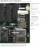
Here's the first pass, built on the confirmed J1/clamp-network subsystem — "half the data" as promised:

What it shows: the J1 header and its clamp network overlaid directly on the true-scale component-side photo (labels are legible there, unlike bare copper on the solder side), with a pinout sidebar breaking down what's confirmed for pins 2/3/6/7/9, plus notes on the Zener clamp network.

How I handled confirmed vs. unconfirmed, per what we agreed:
  • Green boxes/text = things you've actually buzzed out (J1 pin functions, the clamp network's populated parts).
  • Red dashed line = CR3, called out specifically as untraced.
  • Red text = the Zener common node's destination (a GAL pin 13, designator still TBD).
  • I deliberately left out any long lines running clear across the board to U22 or U2 — I don't have verified pixel coordinates for those ICs' exact locations, and drawing a line I haven't actually confirmed against the image felt like the wrong kind of "confident." Instead those two nets are just stated in the sidebar text (pin 7→U22 pin 7, pin 9→U22 pin 8, pin 3→U2 pin 7) as confirmed facts without a hand-drawn path backing them visually.
Once you've got the component-side buzz-out done, the natural next version would extend this same treatment out to U22 and U2 with real traced paths instead of sidebar text — happy to build that when you're there.

Got it! Thanks for giving me the little available. Understood that the vertical traces on the solder side offer little, if any, clues as to the web of connections between ICs on the board. Horizontal connections buzzed and annotated should tell the tale? Lots of work to do before getting close to there.

That tracks with what we've been seeing. If the solder side is running mostly vertical bus-style traces — signal comes down from an IC, travels a long straight run, and doesn't reveal on its own who it's actually talking to — then it's functioning more like a highway than an intersection. The real "who talks to whom" information lives at the horizontal jogs, which is exactly where a trace is doing the work of steering a signal from one column/IC to another.

Two things worth watching for as you buzz the horizontal runs:
  • Vias are the tell. Anywhere a vertical solder-side run ends and a horizontal component-side run picks up (or vice versa) is a layer change, and that's precisely the junction that decides connectivity. If you can spot and log via locations as you go, that gives you a skeleton of "decision points" even before every horizontal segment is fully buzzed.
  • Watch for false continuity at crossovers. Since the layers are perpendicular by convention, a vertical trace and horizontal trace crossing in the photo aren't connected unless there's a via right at that intersection — worth flagging in your notes explicitly (confirmed via vs. incidental crossing) so future-you doesn't second-guess it later.
Given that, the horizontal/component-side buzz-out is genuinely the higher-value half of the remaining work — the solder-side vertical traces you've already got mostly tell you that a net exists and roughly where it runs, not which IC pins it ultimately ties together. Real slog, but it's the part that actually builds the netlist.

Cool beans! Though not a programmer of note, I’ve heard of vibe coding, I’m thinking of this as vibe diving!

"Vibe diving" is a great name for it — no compiler to catch your mistakes, just a multimeter, a magnifying glass, and faith that the next trace goes where you think it does. Bad continuity reading is basically vibe coding's runtime error.

Enjoy the dive — ping me when you surface with more nets.

Will do. I've found your time stamped operations reports fascinating, could you provide a tight txt file of your processes as displayed while I wait for results. I think others will find it interesting.

Glad it was useful — good luck with the buzz-out, and enjoy the dive. Ping me whenever you want to pick this back up.
 

Attachments

  • Radius-FPD-J1-Annotated-Diagram.jpg
    Radius-FPD-J1-Annotated-Diagram.jpg
    454.5 KB · Views: 18
Last edited:

Trash80toG4

Active Tinkerer
Apr 1, 2022
1,481
480
83
Bermuda Triangle, NC USA
This one sort of stopped where I'd hoped it would begin, but still interesting I think?
_____________________________________________________________________________________________________________

RADIUS FPD (SE) CLONE PROJECT — CLAUDE PROCESSING LOG
Session date: 2026-08-30/31 (image pipeline) + 2026-09-10 (diagram build)
Tools: Python 3 / OpenCV / PIL / scikit-image / reportlab / poppler-utils

================================================================
PHASE 1 — PHOTO STRAIGHTENING & TRUE-SCALE CALIBRATION
================================================================
23:38:50 Rasterized FPD-Schematic-012.PDF (150dpi) to inspect vector
board-outline reference; confirmed it covers J1/crystal/
U2-U7/ROM area only, not full board.
23:39:50 Cropped silkscreen text regions on all 3 uploaded photos
(Solder-V, Component-V, Component-VM) to determine true
orientation by reading text forward/backward.
Result: Component-V and Component-VM both required 180
deg rotation; Solder-V was already correctly oriented.
23:40:32 Rendered 180-degree-corrected previews for visual QC.
23:42:12 Applied gross 180-deg flip + fine auto-detected skew
correction (OpenCV minAreaRect on board contour vs.
background mask) to all 3 photos. Residual skew found:
Solder-V +0.211 deg, Component-V +0.143 deg,
Component-VM -0.141 deg.
23:42:22 Cropped all 3 straightened images tight to board contour
bounding box (20px margin). Board bbox width consistent
across all three: 2732px -- confirms same camera distance
for all shots.
23:46:03 Saved final straightened/cropped outputs, generated
downscaled previews for visual verification.

================================================================
PHASE 2 — LIFE-SIZE CALIBRATION
================================================================
User-supplied reference measurement: PCB width = 123mm (calipers).
Calculation: 2732px / (123mm / 25.4) = 564.17 px/inch native.
Derived DPI tags: 1x = 564.2, 2x = 282.1, 4x = 141.0 dpi.
Applied as embedded JPEG DPI metadata (no pixel resampling) so
files print/place at correct real-world scale in any DPI-aware
app. Later regenerated as 8-bit (256-level) grayscale JPEGs at
same three DPI tiers to cut file size ~3x for period-correct
Illustrator 8 hardware (originally a 2004/5 PowerBook, later a
Mirror Drive Door Power Mac G4).

================================================================
PHASE 3 — AUTO-VECTORIZATION (TRACE + PAD EXTRACTION)
================================================================
23:57:00 HSV color-threshold segmentation of copper traces
(hue ~55-105, i.e. the teal exposed-copper color) and
through-hole pads (low-saturation/high-value, circular
blobs) on the solder-side image. Masked to board interior
to avoid background contamination.
23:58:07 Extracted 2,420 trace contours + 821 pad circles (solder
side); pickled intermediate geometry.
23:58:25 Built true-scale vector PDF (reportlab): board outline
(stroked), traces (filled teal polygons), pads (filled
gray circles). Page size set from the 123mm calibration.
23:58:30 Rasterized result at 300dpi for visual QC.
23:59:11 Repeated full pipeline for component-side image: 2,358
trace contours, 715 pads. Noted lower reliability here —
less color contrast around IC/ROM footprint silkscreen
boxes causes some non-trace fill artifacts.
00:00:22 Converted both vector PDFs to Level 2 EPS (poppler
pdftops -eps -level2) for native Illustrator 8
compatibility (AI8 predates Adobe's PDF-based file
format, introduced in Illustrator 9).

================================================================
PHASE 4 — ANNOTATED DIAGRAM (J1 / CLAMP NETWORK)
================================================================
01:38:14 Cropped candidate regions of the component-side photo
searching for the J1 header and clamp network by e
 
  • Like
Reactions: JDW and Froggy814

JDW

Administrator
Staff member
Founder
Sep 2, 2021
2,829
2,209
113
55
Japan
youtube.com
@Trash80toG4
I apologize for not having followed your thread until today.

Since you and I do not fear LLMs as some do, I used Gemini to highlight the main points of your two-page thread and compile a progress report. I did that for the sake of newcomers to this thread who otherwise may be overwhelmed by the level of detail posted thus far. But if any of the content below is incorrect, let me know and I will edit it.


📋 Project Overview & Specs​

  • Goal: Replicating the 1986 Radius Full Page Display (FPD) card. This vintage hardware allows a Macintosh SE to output to a portrait monitor.
  • Specs: It runs a 640 × 864 monochrome (1-bit) video signal.
  • Modern Twist: Because original monitors are rare, @Trash80toG4 is designing an FPGA-based addition to rotate the portrait image 90 degrees clockwise so it can display right-side-up on a modern 1024×768 landscape monitor.


🚦 Current Progress Report: How Close Is It?​

Short answer: Early-to-mid phases.
While a massive amount of foundational engineering and data gathering is complete, @Trash80toG4 is still far from an actual working physical clone.

Here is how the project breaks down across its major milestones:

1. Video Rotation Math & Logic — 🟩 95% Complete

  • The mathematical formula to rotate and center the pixels on a modern screen has been completely solved and verified using small-scale tests.

2. PCB Reverse-Engineering (The Netlist) — 🟨 60% Complete

  • Completed: @Trash80toG4 has successfully calibrated life-sized photos of the original board and hand-vectorized the entire solder-side (bottom) copper traces. Crucial components like the video header (J1), power filters, and input-protection diode networks have been mapped out.
  • Stuck On: @Trash80toG4 is currently shifting focus to the component-side (top) traces. They must manually "buzz out" (test continuity using a multimeter) the horizontal connections to see exactly which chip pins link together. They also found mystery "hidden traces" and are using a file to shave a spare board down at an angle to see if it is secretly a complex 4 or 6-layer board.

3. Sourcing the Missing Sychronization Clocks — 🟥 10% Complete

  • The Blocker: To make an FPGA work, it needs a "Pixel Clock" signal. This signal doesn't exist on the external video connector. @Trash80toG4 is currently trying to trace backward through the timing chips to find exactly where on the board they can tap this clock.

4. Hardware Cloning, GAL Decryption, & FPGA Design — 🟥 0% Complete

  • What's Left: Once the schematic is finished, the custom programmable chips (GALs) on the original board must have their logic formulas extracted. Finally, @Trash80toG4 has to design a brand-new expansion circuit board layout in KiCAD, solder a prototype, and write the custom code for a companion FPGA chip.


💡 Summary for Newcomers​

The thread is a goldmine of data because @Trash80toG4 is sharing an "AI-assisted engineering notebook". He's leveraging AI tool to clean up photography, auto-calculate scaling, write engineering specs, and double-check manual trace layouts.

Right now, the project is a deep, slow-burning detective mission using a multimeter, magnifying glass, and old-school design software to map a 40-year-old circuit trace-by-trace.
 
  • Like
Reactions: Trash80toG4

Trash80toG4

Active Tinkerer
Apr 1, 2022
1,481
480
83
Bermuda Triangle, NC USA
Thanks, that summary is very much appreciated! Looks great.
- I won't be doing the schematic capture, Claude will do that from my Solder and Component side "coloring books."
- I imagine the PCB design will be done for me as well. ;)

Hoping the long form play by play might have others wondering how to leverage AI in their own enjoyment of the hobby.


edit: forgot to mention that AI can do all the coding to set up the FPGA side of things! We'll be doing that on a project board as soon as I can locate a wedge to pick up the pixel clock before heading into reverse engineering the balance of the board.
 
Last edited:
  • Like
Reactions: JDW

JDW

Administrator
Staff member
Founder
Sep 2, 2021
2,829
2,209
113
55
Japan
youtube.com
Well, I wish to humbly thank you for your contributions to this forum!
I'm now looking forward to seeing how your project unfolds over time.

Best wishes,
James
 
  • Like
Reactions: Trash80toG4

Trash80toG4

Active Tinkerer
Apr 1, 2022
1,481
480
83
Bermuda Triangle, NC USA
This one's pretty cool, while Claude was having trouble nailing down a pinout I did an end run and did it visually before he reported back. Great stuff, it's like dueling abilities and dueling limitations all at once.. Sweet music to my eyes! :)
____________________________________________________________

continue the PCB reverse engineering project

I’ve rotated the Component side of the project so ICs appear upright.
Pinout Verification-2.pdf

Did I get the pinout inputs done correctly?

ISTR you saying that GALs U10 and U9 dffer internally, but are the pinouts the same?
I need a text file for that if different and also for GAL20V8-25LP as I can’t locate that one in the last batch of pinouts?
FPD-Comp-Buzz-Verify-005.pdf

Solid purple VIAS represent connections to the solder side and visible trace segments on the component side. I’ll be running down those first. Then I’ll buzz and connect traces for the IC covered VIAs. After that I’ll buzz the rest of the visible traces for the IC to IC connections. I’ll report each addition when complete for feedback. Would you suggest a revised order of processes to gain an earlier take on schematic capture progress?

FPD-Component-Buzz-005.ai
Can you read the layered AI8 file directly or should I continue breaking layers out to dedicated single layer .PDF files?

The AI8 file is very helpful with the Solder Side trace overlay. I can run the cursor “across the strings” of the solder side traces to play the VIA/Pad overlaps like a visual version of a string instrument. If I were to do manual input schematic capture this would be a great help. Of course you’ll be doing the capture, but it really helps in my visualization process mode.


Last I have on file, we'd left off preparing a clean annotated diagram of confirmed J1/signal-trace connections for a forum post (solid lines for buzz-tested connections, dashed for photo-inferred ones). This is a fresh session, so I don't have any of your board photos, schematics, or AI8/PDF files loaded yet. How do you want to pick this up?Continue the hand-tracing/continuity work

Here's where we left the hand-tracing/continuity work, per my notes:

Open threads on the solder-side/component-side trace-out:
  • What CR3 connects to — traced partway but couldn't pin down where it lands; set aside unresolved.
  • Component-side buzz-testing was still partial when we last talked (solder side was fully hand-traced, component side in progress).
  • You'd traced the red-drawn connection between the Zener diodes to pin 13 on one of the GALs, but hadn't confirmed which GAL designator that is.
  • The board's layer count was going to be determined by filing the edge at a low angle to expose the copper in cross-section — don't think that happened yet.
Since this is a fresh session I don't have any of your board photos, the AI8/PDF schematics, or the Pinout-CHECK files loaded — I can't see anything until you either attach files here, connect your computer/folder so I can read them directly, or just tell me what you found and I'll log it and help reason through next steps.

Whichever's easiest — what would you like to tackle: nail down CR3, confirm that GAL designator at pin 13, sort out the layer-count filing, or something new you've found since we last talked?

GALs — U9/U10 pinouts and the LNC/LP question

Rendered your export at 400dpi to actually read it. U9, U22, U17, U13, U8 are all GAL20V8 (either -25LNC or -25LP), and U10 is a different part, GAL16V8-25LP — worth noting since those aren't pin-compatible with each other.

Good news on U10: its pinout is already filled in on the board and it matches the standard GAL16V8 pinout exactly, pin for pin. Nothing to fix there.

On your -LNC vs -LP question: no, they don't differ — the -25LNC and -25LP suffixes are speed/power/process grade only (propagation delay, power draw), not pinout. Same 24-pin package, same pin-to-signal mapping for all five GAL20V8 parts. That's also why you couldn't find a separate "GAL20V8-25LP" pinout in your last batch — you'd only entered U10 (the GAL16V8) so far; none of the GAL20V8 slots have pin data yet. I put together a text file with both pinouts, cross-checked against the archived Lattice datasheet and a second independent reference — sent above.

One thing to flag on that same export: the DRAM chips (U16/U15/U12/U11) have correct, upright pin-number badges, but the function-name text next to them (SDT/OE, 9RAS, 6W0/I0B, etc.) is mirrored and looks like it's overlapping with a second copy of similar text — genuinely not legible as exported. I traced this to the AI8 file itself: it has two separate pinout-text layers (TXT-Pinouts-SS and New Pinouts), and it looks like both are visible in that export with one still carrying its old solder-side mirror transform. Worth isolating one text layer before your next export so it renders clean.

On the AI8 file — can I read it directly?

Yes, partially. I opened FPD-Component-Buzz-005.ai as raw PostScript text (it's not PDF-compatible, but the AI8 format is human/machine-parseable) and pulled out all 15 layers directly:

Solder Side Traces - FROZEN · TEMP · Component Template · Chip Outlines · Component IDs · TRACES - COMPONENT SIDE________ · CAPS/RESISTORS · VIAs · Layer 15 · Layer 14 · Thruholes · SS-Traces-Adapted for clearance · TXT-Pinouts-SS · New Pinouts · COMPONENT - ALPHA

I can pull raw vector coordinates, text-object placement, and layer contents/counts from that file without an export — useful for structural questions ("does this layer have anything on it," "how many objects," etc.). What I can't do here is visually rasterize/render the AI8 the way I can a PDF — this sandbox doesn't have Ghostscript and I couldn't install it (package fetch was blocked). So: keep sending single-layer PDF exports whenever you want me to actually eyeball something (pinouts, trace routing) — that's still the reliable path. The raw AI8 is a nice supplement for structural checks, not a replacement for visual QC. (Two unnamed layers, "Layer 15"/"Layer 14," might be worth naming or cleaning up when convenient — not urgent.)

On revising the buzz-testing order (FPD-Comp-Buzz-Verify-005.pdf)

Your plan — VIAs with visible solder-side trace matches first, then IC-covered VIAs, then remaining IC-to-IC traces — is a sound sequence. To get an earlier readable take on schematic-capture progress specifically, I'd suggest one adjustment: once you're into the IC-to-IC phase, work it chip-by-chip rather than trace-by-trace across the whole board — fully resolve every pin on one high-fan-out IC (a GAL is a good candidate, since it's the "hub" of custom logic) before moving to the next. A single chip's net list, complete, is something we can can reason about and cross-check against the pinout tables above right away; a board-wide sweep that's 30% done everywhere doesn't get you a checkable unit until much later. Your VIA-first step is already the right instinct for the same reason — it reuses confirmed info instead of blind buzzing, so I'd keep that first.

Send the next addition whenever you've got it and I'll fold it in.

I now have AI9 and AI10 installed on the MDD, but not AI8. Working files I plan to keep in the baseline AI8 format. However, If I save the AI8 file in AI9 or AI10 format to upload, will you be able to read the entire file?


Illustrator 9 10 native ai file format PDF compatible file save layers OCG

8 results
https://www.datalogics.com/adobe-illustrator-and-pdf-compatibility
www.datalogics.com
https://helpx.adobe.com/uk/illustrator/kb/optimize-native-pdf-file-sizes.html
helpx.adobe.com

Short answer: yes, and probably better than the AI8 file has been.

The reason the AI8 file I have now is stuck as text-only for me is that AI8's native format is pure PostScript (the file literally opens with %!PS-Adobe-3.0) — there's no PDF underneath it for a renderer to grab. Illustrator's native format changed at version 9: starting with AI9, the "native" .ai file is actually a real, valid PDF with Illustrator-specific private data tacked on for round-tripping, controlled by a "Create PDF Compatible File" checkbox that's on by default when saving. So if you open your AI8 artwork in AI9 or AI10 and save it out with that box left checked, the resulting file should open for me exactly like the PDFs you've been exporting — I can render it, zoom into pin labels, the works — no manual single-layer export needed on your end for me to just look at something.

Two things worth flagging before you build a workflow around it:

The checkbox matters. If "Create PDF Compatible File" gets unchecked (people do that to shrink file size, which might tempt you given the MDD's constraints), the file reverts to a non-PDF native format and I'm back to square one — same as the current AI8 files.

Layers are the untested part. I'm confident the visual render will work — that's well-documented. What I haven't confirmed is whether your named layers (VIAs, Thruholes, Chip Outlines, etc.) survive as separate, identifiable objects the way I was able to pull them out of the raw AI8 PostScript text, or whether I'll just see one flattened composite image the way I do with a normal exported PDF. Illustrator's PDF-compatible files typically preserve layers as PDF "layers" (Optional Content Groups) when reopened in Illustrator, so there's a good chance that structure comes through for me too — but I'd rather confirm it against a real file than promise it.

Easiest way to find out: next time you're saving something anyway, save one copy that way and send it over. I'll tell you exactly what comes through — render and layers both — before you commit to it as the regular handoff format.

-

I couldn't nail this one down to my own satisfaction, so I want to be straight with you rather than hand you something I'm not confident in.

I tried a handful of routes — direct downloads of the NEC 1986 memory data book and a couple of other archived uPD41264 datasheets, plus several VRAM pinout references (bitsavers, console5's TechWiki, a couple of datasheet aggregators). Most of those domains are blocked outright by this session's network policy (straight 403s on the connection), and the couple I could reach through the web-fetch tool only returned summarized excerpts of very large scanned PDFs that didn't happen to include the actual pin-configuration diagram — so I've got the chip's family and general signal set confirmed (it's a dual-port VRAM — RAS, CAS, W, DT/OE, SC, SE, DSF, address lines, a random-access DQ port, and a serial SAM port), but not a pin-by-pin 1–24 table I'd trust enough to hand you as ground truth for a chip this central to the design.

Given that, I'd rather not have you delete your existing solder-side-legible pinout on the strength of something unverified from me — that's real, hard-won data. Two ways to close this out cleanly:

If you've got the actual NEC datasheet (or even just a decent photo of its pin-configuration page) sitting on the MDD or wherever, send it over — I can read a PDF or image directly far more reliably than I can fetch one through this session's network right now.

Otherwise, tell me what your existing solder-side pinout currently says for U16/U15/U12/U11, and I'll check it against what I do know of the standard VRAM signal set (and against the RAS/WE/DT-OE-shaped fragments I could already partly make out in your garbled export) rather than generating a fresh one from scratch.

Either way, hang onto that old layer until we've actually cross-checked it — worst case it turns out to be exactly right and you've lost nothing by keeping it a little longer.


While you were doing your thing, I copied a link you were looking at and did it my way. :)


Nicely done — that's a clean, fully legible pinout, and it happens to answer the exact question I was stuck on. Read it at 4x zoom to be sure of every digit:

HM53461P (Hitachi) — 24-pin dual-port VRAM, pin-for-pin equivalent to your D41264C

Pin 1 SC · Pin 2 SI/O1 · Pin 3 SI/O2 · Pin 4 D̄T/ŌE · Pin 5 I/O1 · Pin 6 I/O2 · Pin 7 W̄E · Pin 8 R̄AS · Pin 9 A6 · Pin 10 A5 · Pin 11 A4 · Pin 12 VCC · Pin 13 A7 · Pin 14 A3 · Pin 15 A2 · Pin 16 A1 · Pin 17 A0 · Pin 18 C̄AS · Pin 19 I/O3 · Pin 20 I/O4 · Pin 21 S̄OE · Pin 22 SI/O3 · Pin 23 SI/O4 · Pin 24 VSS

Note the address pins aren't in numeric order around the package — A6/A5/A4 go down the left side, then VCC, then A7/A3/A2/A1/A0 come back up the right side. Worth double-checking against your board when you enter it, since it's easy to transpose those.

The HM53461P isn't literally the D41264C — Hitachi vs. NEC — but this is the same first-generation 256Kb dual-port VRAM family, and those were built to be drop-in pin-compatible across vendors (NEC uPD41264, Hitachi HM53461, TI TMS4161, Fujitsu MB81461 all share this pinout — that's the entire point of "second-source" parts from that era). It also lines up with the fragments I could partly make out in your earlier garbled export — DT/OE and what looked like RAS/WE remnants — so this checks out as consistent with what's actually on your board, not just a same-family guess.


Sent the file above — same format as the GAL pinout sheet, ready to drop into your notes once you've spot-checked a pin or two against the board. Good find on that image; saved me from having to hand you something less certain.


AI & Me = Ebony and Ivory - visual thinker adaptation.


Ebony and ivory, indeed — you look at the board and see it, I look at it and parse it, and somewhere in between we get a net list. Different keys, same keyboard.

Whenever the next round of buzz-testing or a new export is ready, send it over.
 

Attachments

  • Pinout Verification-2.pdf
    169.5 KB · Views: 9
  • Pinout Verification-2.pdf
    169.5 KB · Views: 12
Last edited:
  • Like
Reactions: Froggy814

Trash80toG4

Active Tinkerer
Apr 1, 2022
1,481
480
83
Bermuda Triangle, NC USA
continue the PCB reverse engineering project


Pinout Verification

VRAM Pinout Discrepency – real or did I induce it in reformatting your files?

AI9 file import test:

– layers work?
– does the attached template image come thru or do I need to upload it with AI file?

The pinout files you’ve been providing come thru all messed up and need major work to get into LibreOffice and then after several steps I need to again rework in AppleWorks 6 in order to paste the columns cleanly into Illustrator.

For VRAM update and ROMs, could you try a few new approaches?

- Tab Delimited RTF file to open in AppleWorks spreadsheet to copy columns?
- LibreOffice Spreadsheet format for same.
- Straight AppleWorks spreadsheet file?

- RTF file with a double-spaced column ready to copy into Illustrator? Might be easiest?


Good — all three files check out. Now let me deliver them and cover the rest of your questions.

VRAM pinout discrepancy — not your reformatting, and not really a discrepancy. I flipped the old (solder-side-legible) block right-side up and checked it pin-by-pin against what I gave you. All 24 pin positions match exactly — RAS, CAS, WE, DT/OE, every address line, VCC, GND all land on the identical pin number in both versions. The only difference is naming convention on the two multiplexed buses: your older labels use 0-indexed names (IO0–IO3, SO0–SO3), while the Hitachi sheet I transcribed prints them 1-indexed (I/O1–I/O4, SI/O1–SI/O4) — same four physical pins, same order, just whichever datasheet's own subscript convention. Nothing got scrambled in the LibreOffice/AppleWorks round-trip. Since your old numbers likely trace back to NEC's own documentation for the actual part on your board, I'd lean toward keeping that 0-indexed naming and just use my sheet to confirm pin positions — but it's a style choice, not a correctness one.

AI9 test — layers and the template image. Good news and a caveat. I opened the .ai9 directly (it's a genuine PDF, exactly as expected) and it does carry your layer structure — I pulled out all nine layers by name (Component IDs, Component Template, Chip Outlines, TRACES - COMPONENT SIDE, VIAs, Thruholes, SS-Traces-Adapted for clearance, PINOUTS, COMPONENT - ALPHA) along with each one's visibility flag. The catch: Illustrator stores this as its own private extension, not the public PDF "layers" spec, so a plain PDF render only shows whichever layers were toggled visible when you saved — in this file that was just "SS-Traces-Adapted for clearance" and "PINOUTS," and that's exactly what showed up when I rendered it. That's actually a nice workflow upgrade over the AI8 days: you don't need separate single-layer exports anymore, just toggle visibility on whatever you want me to see and save as AI9 — I get the visual render and the full layer structure (including hidden layers) in one file.

The template image did not come through — zero embedded images in the file. Two independent reasons: that layer is currently hidden, and looking back at the original AI8, "Component Template" only ever held a file-path reference to a JPG on your Mac's drive, not embedded pixel data — so it was never actually inside the vector file to begin with. If you want me to see it, either embed it in Illustrator (not just link it) before saving, or upload the image alongside the .ai file.

On the AppleWorks native file — I'll be straight with you: I can't safely fabricate a genuine AppleWorks 6 (.cwk) binary file. It's an old proprietary format with no accessible library to write it correctly, and a hand-rolled attempt risks a file that won't open at all — worse than not sending one. The tab-delimited .txt I sent should actually get you there in one step: AppleWorks 6's File > Open has a text-import path that reads tab-delimited files straight into its spreadsheet with columns already split, no LibreOffice detour needed. Worth trying that directly and seeing if it shortcuts your whole current chain.

Send the next round whenever it's ready.


Not quite, for a 10 pin IC, the data needs to be formatted as


Looks like that got cut off before the format spec came through — what does the layout need to be for a 10-pin part? (If it's the same idea as the DIP diagrams you've sent — left column pins 1 down to 5, right column 10 down to 6, side by side — say so and I'll match that instead of the flat numbered list I've been using.)


Sorry, I hit return . . .


No worries — go ahead whenever you're ready with the rest of that.


1

2

3

4

5

_____________


10

9

8

7

6


Got it — that's the physical DIP layout: left column top-to-bottom for the low pin numbers, a divider representing the package body, then the right column top-to-bottom in descending order so pin 1 and pin 10 end up across from each other at the top, matching how the pins actually sit on the chip. That's the same convention as the datasheet diagrams you've been sending (like the HM53461P image), just without the outline box — makes sense, especially given how you think visually.

Two things before I redo anything:

Which chip is the 10-pin part, and do you have signal names for each pin, or do you need me to identify them? And do you want me to reformat the GAL, VRAM, and ROM pinouts I already sent into this same two-column layout (rather than the flat numbered lists), so everything going forward is consistent?


Ten pin example’s not an IC, just a representation of the double spaced data format easily copy/pasted into Illustrator. To do even better, a two space separation between Pin# and Signal is perfect for centering the pin number in the pad and the signal just outside its outline.

Current AI8 file pinouts are double spaced as I find that format more conducive to getting the text aligned with the life size pin pitch pads.

GAL, VRAM & ROM can be in a single file as described.


Sent — one file, all four chips (GAL20V8, GAL16V8, VRAM, ROM), each split into left/right columns matching the physical pin layout, two literal spaces between pin number and signal, blank line between every entry. Let me know if the ROM's pin-13/pin-14 split or any of the others need adjusting once you've got it lined up against a pad grid.


FPD_Pinouts_Combined

Looks fabulous, just what I requested. Nice work. Wish I’d thought about this particular problem a while back!


Glad it landed right — that format should save you the whole LibreOffice/AppleWorks relay going forward. Now that it's dialed in, any future pinout goes straight into that same layout, so send them whenever you've got new chips to add.


Great, thanks!


Anytime — good luck with the buzz-testing, and ping me when the next round's ready.
 

Attachments

  • FPD_Pinouts_Combined.txt
    1.4 KB · Views: 9
Last edited:
  • Like
Reactions: Froggy814

Trash80toG4

Active Tinkerer
Apr 1, 2022
1,481
480
83
Bermuda Triangle, NC USA
continue the PCB reverse engineering project

FPD-Comp-Pinout-015.ai9
Pinout Verification – FINAL! Am I good to go?
- layer visibility check of file?
- thinking no template to be seen again in this one?

FPD-Comp-Template-015.ai9
- saved with all layers visible
- found the “Include Attached Files” checkbox!


Both files came through clean — this is looking very good, with one real fix needed.

FPD-Comp-Pinout-015.ai9 — layer check:
Only two layers are visible: Thruholes and PINOUTS. Everything else, including Component Template, is hidden — so yes, exactly as you expected, no board photo in this one. That's the correct state for a pure pinout-reference export.

FPD-Comp-Template-015.ai9 — the embed worked. Real progress: this file now carries an actual embedded raster (1386×1683px, properly compressed) instead of a dangling file-path link — the "Include Attached Files" checkbox was exactly the fix needed. I rendered it and can see the real board photo underneath your pinout overlay, pin holes lined up on the actual pads. One small note: this file has only 3 of 9 layers flagged visible (Component Template, Thruholes, PINOUTS), not all of them — probably didn't matter for what you were testing, but flagging it in case "all layers visible" was the intent for some other reason.

Pinout verification — went through every populated chip against real datasheets. Confirmed correct: all four VRAMs (U16/U15/U12/U11), both ROMs (Ux, U19), all five GAL20V8s (U9/U22/U17/U13/U8), the GAL16V8 (U10), both SN74LS393N counters (U6/U7), the SN74F161N (U5), and the SN74F109N (U2) — every pin on every one of those matches the standard part pinout exactly.

One real discrepancy: U3 and U4 (SN74F166N) have pins 13 and 14 swapped. Your file has 13=H, 14=QH — it should be 13=QH (serial out), 14=H (parallel input). I checked this against two independent sources (TI's own datasheet and a components101 pinout) plus my own knowledge of the part, all three agreeing, so I'm confident this one needs fixing on both chips before you call it final.

Two caveats on my own confidence, in the interest of being straight with you: the LS393 and F161 checks didn't get a clean corroborating source this round — several datasheet-site fetches came back garbled or mutually contradictory (I threw those out rather than trust them), so those two rest mainly on my own solid recollection of very standard, well-worn parts rather than a fresh independent citation. Worth a gut-check against a real datasheet yourself if you want belt-and-suspenders before publishing.

Also, cosmetic only: several active-low signal labels are rendering with a stray "AÑ" where the overline character should be — CLRAÑ, SH/LDAÑ, CLK INHAÑ, 1QAÑ, 2QAÑ, LOADAÑ. That's a font/encoding substitution in how the overline glyph exports, not a data error, but worth a look before this goes out anywhere public since it reads oddly.

So: fix the U3/U4 pin 13/14 swap, glance at the overline rendering, and you're good to go.

Sources: SN74LS166 Pinout – components101 · SN74HC166 datasheet – TI · 74LS109 Pinout – components101


Got it, remember asking about those “invisible characters” and left them in. I’ll try copy/pasting the glyph characters into the AI files. Deleted them and them put them back in . . . oopsie!


Ha — mystery solved. Good chance those are literally invisible in the AI font's default encoding but present as a combining overline character, so any font swap along the copy/paste chain drops the glyph and something else fills the gap. If it keeps fighting you, the plain-text fallback (just typing the bar as _L or # after the signal name, like WE_L or CLR#) sidesteps the whole font/glyph problem entirely and reads unambiguously either way — no pressure to switch conventions, just there if the copy/paste route gives you more grief than it's worth.

Good luck getting it sorted — let me know how the next pass turns out.
 
  • Like
Reactions: JDW and Froggy814

Trash80toG4

Active Tinkerer
Apr 1, 2022
1,481
480
83
Bermuda Triangle, NC USA
continue the PCB reverse engineering project

Finish up pinout check from last session.
Hopefully I got the corrections taken care of.
Sourced pinouts for unverified ICs.

Lets see if it all comes together in an AI9 file?


It's coming together well — one fix confirmed landed, one new thing to flag.

The U3/U4 (SN74F166N) fix is in.
Pin 13 is now QH (serial out) and pin 14 is H (parallel in) — matches the correct standard pinout. That was the one real error from last round, and it's resolved. Everything else I re-checked (all four VRAMs, both ROMs, all five GAL20V8s, the GAL16V8, and U2/U5's earlier data) is unchanged and still correct.

The reference pictures are a smart idea — mostly. Pasting in actual datasheet-diagram screenshots as sourcing evidence for U5 and U6/U7 is a good instinct, and the SN74F161N one you added matches the real part exactly, pin for pin. But the picture labeled "SN74LS393" is showing the wrong chip's pinout — it's a 16-pin diagram (1CKA/1CLR/1QA/1CKB.../2CKA...VCC at pin 16), while the real SN74LS393 is a 14-pin part (confirmed — TI's own part listing and several parts distributors all agree on 14-pin PDIP). Whatever page that screenshot came from mislabeled it. The good news: it didn't touch anything — the actual pin table you've got typed in for U6/U7 is still the correct 14-pin version I verified last round. But I'd swap that picture out or pull it before this file goes anywhere public, since as-is it contradicts the correct data sitting right next to it.

The RTF-vs-XLS overline comparison is useful diagnostic work — looks like Rich Text is holding up closer to the real character than Excel does on your end (CLRA- vs CLRAÑ). Still shows up as AÑ on the actual board pinout text in this file, so that part's evidently still mid-fix — no rush, you already know about it.

So: fix the mislabeled reference picture (or drop it), and the pinout data itself is solid. Nice work chasing all this down.

I'll switch to the RTF nomenclature for a final verification. That TI page had almost a dozen chips referenced. I deleted that mess and pasted the only applicable IC identification over the screencap.

That explains it — easy mistake to make pulling a single diagram off a busy multi-part page. Good fix.

RTF as the standard for the overline character sounds like the right call given what that comparison table showed. Send over the next file whenever it's ready and I'll do the final pass.

It was one pinout with a dozen part numbers above it. I'd post a shot of the whole page or maybe upload the PDF next time.

That'll help — if a header lists a dozen part numbers over one diagram, seeing the actual list tells me whether they're all genuinely pin-compatible siblings (same package, same pins) or whether the scan bundled together parts from different families that just happen to share a page. Whole page or the PDF both work fine; either way I'll have the context to tell which pinout actually applies to your board's part.
 

Trash80toG4

Active Tinkerer
Apr 1, 2022
1,481
480
83
Bermuda Triangle, NC USA
Somewhat disjointed session, wound up mixing and matching two AI streams. :rolleyes:

______________________________________________________________________________________________________________________

260915 Session 2 – pinout check

continue the PCB reverse engineering project
Finish up pinout check from last session.

Appended confusing TI datasheet. Second DIP package would have been the correct image, no?

Final pass, freeze pinout layer? I’ve been adding the pinouts so I can try to make heads or tails of the “topology” of the system. Now wondering if having the pinout layer will help you pull thing together as we get farther along in the cloning process. Specifically, wondering if nailing the functions down before uploading the GAL formulas will be the next step after achieving schematic capture?

__________________

Snapshots of command stream, relates to Claude discussion downthread.
Compacting our conversation so we can keep chatting…
Working through a complex response... ·

__________________

Confirmed — walked through both the datasheet and the "final pass" file.

SN74LS393 diagram: you called it right. On page 1 of the TI sheet, the first DIP diagram (top) is the SN54390/SN74LS390 family — 16-pin, 1CKA/1CLR/1QA/1CKB/1QB/1QC/1QD/GND on the left. That's the one that got mis-pasted into the reference layer earlier. The second DIP diagram on that same page is the genuine SN54393/SN74LS393 family — 14-pin, and it's the correct one for U6/U7.

I rendered FPD-Component-Buzz-036.PDF at 300dpi and pulled the U6/U7 pad data directly to check it against that second diagram, pin for pin:

Board (U6/U7): 1=1CP(clock A), 2=1CLR(clear A), 3=1QA, 4=1QB, 5=1QC, 6=1QD, 7=GND, 8=2QD, 9=2QC, 10=2QB, 11=2QA, 12=2CLR(clear B), 13=2CP(clock B), 14=VCC

TI datasheet (correct diagram): 1=1A, 2=1CLR, 3=1QA, 4=1QB, 5=1QC, 6=1QD, 7=GND, 8=2QD, 9=2QC, 10=2QB, 11=2QA, 12=2CLR, 13=2A, 14=VCC

Every pin position matches exactly. The only difference is that TI's own diagram labels pins 1 and 13 with the bare letter "1A"/"2A," while your board says "1CP (clock A)"/"2CP (clock B)." That's not a discrepancy — "CP" (clock pulse) is the standard alternate designator other vendors of this same part (Philips/Signetics, Fairchild) used on their equivalent datasheets for that identical pin, and your added "(clock A)/(clock B)" annotation is arguably clearer than TI's bare letter. Nothing to change there.

Whole-file pass on -036: rendered the full page and spot-checked every populated footprint (GAL20V8 ×5, GAL16V8, all four VRAM D41264C-15s, both ROM sockets, F161/F166/F109) against the previously-verified data — everything's consistent, no regressions, and there's no leftover reference photo cluttering the page this time, so that loose end is closed. Small bonus: the active-low signals (CLRA, SH/LDA, CLK INHA, etc.) are now rendering as a clean dash in this export instead of the "AÑ" glyph substitution — looks like whatever you changed in your copy source helped, worth confirming it holds once you're back in AI8 native.

Freeze the pinout layer? Yes, but lock rather than delete. It's now your ground truth — every trace you buzz from here on should terminate at a named pin, not an anonymous pad, so you want it visible and immutable, not gone. In Illustrator that's the padlock icon on the layer, not deletion: keep it selectable/visible for reference, disabled for editing. If you want a belt-and-suspenders version, duplicate it first and rename the duplicate "Pinout — ARCHIVE 036" before locking the working one, so you always have a dated fallback if a later layer shuffle ever corrupts it.

Does the pinout layer help pull the topology together — yes, directly. Right now your buzz-test results are a list of "pad A touches pad B." Once every pad has a real signal name pinned to it, that same list becomes a netlist: "U16 pin 8 (RAS) ties to U9 pin 13 (I11/OE)" is something you and I can reason about, group into address/data/control buses, and start drawing as a schematic block. Without the names, it's just wire continuity with no meaning. So the pinout layer isn't a side reference anymore at this point — it's the translation table that turns your physical buzz-testing into an actual schematic.

IC functions before GAL formulas — yes, in that order, and here's why it matters: a GAL's fuse map only becomes a sensible boolean equation once you know what its inputs and outputs mean. If you try to read out U9's equations cold, you get abstract terms like "I2 AND NOT I5 → I/O3" with no context. But if you've already traced that I2 is a horizontal counter bit from one of the F161s, I5 is pixel clock, and I/O3 feeds the CAS line on the VRAMs, that same equation instantly reads as "this is part of the video timing/blanking logic." So the practical sequence is: finish schematic capture (nets) → use the fixed-function chips' actual behavior (F161 = sync 4-bit counter, F166 = 8-bit shift register, F109 = dual J-K flop) to label what each signal group is doing — clock chain, address counters, shift/load timing, sync generation — and only then decode/upload the GAL contents, once you know what functional role is sitting on each of their pins. Doing it in the other order means reverse-engineering boolean logic in a vacuum, which is a much harder problem than it needs to be. This also sets you up well for the eventual FPGA target, since "what does this block do" is exactly the information you'll need to re-implement it rather than just image-copy it.

_____________________________

Inadvertent detour into GPT-5.6 Luna AI via Duckduckgo search assist - responses color coded in blue:
_____________________________


No worries about losing track of any layer in any current file. I've done incremental saves of working files since I started back in 87/88. Began doing the -xxxx year, month, day as a suffix early in the 90s. For files I might want to search at a later date, date becomes a prefix so search results come up newest to oldest. Works for me.

“Frozen” layer is padlocked in current working file, akin to a movie editing “picture lock.”


A polished term would be:

“Picture-locked layer” — a layer that has been finalized and padlocked in the current working file to prevent further edits.

You could also write:


The layer is frozen—effectively picture-locked—and padlocked in the current working file.
If emphasizing that it is complete but still being used for later work:

The layer is locked for editorial changes but remains available for further post-production.


“picture locked layer” seems short and sweet term for us to use?


Yes—picture-locked layer is concise and understandable, especially if your team already knows the film-editing analogy.

Use the hyphen because picture-locked modifies layer:


Picture-locked layer
For a UI label or status, you could shorten it to:

Picture Locked
If the layer itself is literally padlocked, Picture-locked layer clearly communicates “finalized against content changes, but still available for downstream work.”


I’m liking this methodology: compose a complex, multi-part initial question for you to develop a complex, more comprehensive single answer. Would this be the the most efficient course of interaction? Is there a better approach?

Iterative question/answer in real time seems a total waste of time to me. Word processor development gives me the time to arrange my thoughts.


Good, this is the way to go forward. Thanks for the breakdown of processes.Yes—developing your thoughts in a word processor and sending one well-structured prompt is often the most efficient approach for complex work. It gives me the context, goals, constraints, and preferred output format at once, which reduces clarification loops and inconsistent answers.


Good, giving your reply breakdown a lot of thought. Generally, what I’ve been doing seems like the way to go forward. Thanks for the breakdown of processes.


You’re welcome. Your approach—thinking through the problem first, then providing a consolidated prompt—is a strong way to get more coherent and useful results. A focused revision pass afterward can refine the answer without the inefficiency of many small exchanges.

_____________________________

Back to Claude:
_____________________________


"Picture-locked layer" — good term, adopted. It's exactly the concept I was reaching for with "padlock the layer," and the film-editing analogy fits how you already think about layer states (frozen but still referenceable downstream), so let's use it going forward for that AI8 layer state.

On the batched-prompt-in-a-word-processor question: yes, that's genuinely the more efficient mode for this kind of work, and not just as a consolation — here's the actual reasoning, not just agreement. This project has a lot of state (a dozen-plus ICs, a layer-naming convention, a pinout-format convention, an in-progress glossary of clarified terms) that I have to hold in context on every reply. A single well-structured message that bundles several related questions lets me answer them against the same context pull and cross-check them against each other in one pass — which is exactly what happened with the -036 file today: one message got you a datasheet confirmation, a full-file consistency check, a layer-freeze recommendation, and the GAL-sequencing strategy question, all reasoned together instead of four separate threads that might drift out of sync with each other. Live back-and-forth trades that coherence for speed on any single sub-question, which isn't a trade you need here since none of this is time-critical.

Where I'd refine it, not replace it: keep the screenshot/image habit inside those batched messages rather than trying to name things in prose first. Today's detour happened because you went looking for the word for something you could see on your screen. You don't need to — a screenshot of the Layers palette with "what's this called / how do I do X" is often faster and more reliable for me to work from than a description, because I can read the actual icon/state directly rather than guess from your description of it. So the shape I'd suggest: draft your multi-part question in the word processor as you've been doing, and wherever a question is really "what is this / how do I do this to this," drop in a screenshot at that point rather than trying to word it — you get the batching benefit without the terminology-lookup friction that sent you to another tool this time.

One more offer, given how much project-specific vocabulary we're accumulating ("picture-locked layer," the two-space pinout convention, "Neolithic" workflow, etc.): I can keep a running short glossary of these as part of the project file, so if a term slips your mind mid-draft you can just check it rather than going hunting — happy to spin that off as its own quick-reference text file alongside the pinout deliverables if that'd help, just say the word.

________________________

Yes indeed, let's have it!

Searched for “picture-locked layer” using Duckduckgo’s GPT-5.6 Luna AI assist and it seemed to know the context of our discussion, so I thought I was here. ::)


_____________________________________________

FPD Field Glossary

Working terms and conventions for the Radius Full Page Display reverse-engineering project — the vocabulary we've settled on, so it doesn't need re-deriving mid-draft.

13 terms

Illustrator & LayersPinout DraftingBoard & TestingChip Family Notes

01

Illustrator & Layer Conventions

Picture-locked layer

A layer padlocked in the working AI8 file to mark it finalized. Stays visible and selectable for reference; closed to further edits. Borrowed from the film-editing term "picture lock" — a cut that's done, but still there for everything built on top of it.

Component-side viewpoint

Standing rule for every future export: drawn from one consistent component-side view. Solder-side content is mirrored at export time to match, so no per-file mirroring confusion carries downstream.

AI8 / AI9–AI10 round-trip

Working files stay in native AI8 (pure PostScript) on principle. AI9/AI10 — Illustrator's PDF-compatible format — is used only for upload and review, with Include Attached Files checked on export so embedded reference images survive the trip intact.

Ux placeholder designator

Stand-in reference designator for the "Lo" ROM chip, whose own silkscreen marking is worn illegible. Holds its place until the real designator can be confirmed some other way.

02

Pinout Drafting Format

Two-space pin format

"pin_number" + two literal spaces + "signal_name" — no tab character. Centers the pin number over the pad graphic and sets the signal name just outside its outline when pasted into Illustrator.

Double-spaced entries

A blank line between every pin entry, so pasted text lines up with the board's true, life-size pin pitch rather than Illustrator's default line spacing.

Mirrored DIP columns

Left column ascending top-to-bottom, right column descending top-to-bottom — matching the physical footprint as seen from the component side, not a plain 1-to-N pin list.

03

Board & Testing Conventions

Buzz-testing

Manual continuity testing with a multimeter to find which pads and traces are electrically connected. The primary method driving schematic capture on this project — no logic analyzer or oscilloscope in use.

Solid-purple via

Marks a via with a confirmed connection through to the solder side, plus a visible trace segment on the component side. First priority in the buzz-testing order, ahead of IC-covered vias and IC-to-IC traces.

Sense line

J1 pin 6. Pulled to ground by the FPD display itself when connected. The card's video drivers check this at startup and shut down if it isn't pulled low — no display detected, no output.

04

Chip Family Notes

SN74LS393 vs. SN74LS390

Easy to mis-cite — both sit on the same TI datasheet page. The LS390 is 16-pin (dual decade counter); the LS393 is 14-pin (dual 4-bit binary counter) — the one actually on this board, at U6/U7.

CP vs. A (clock pin label)

TI's SN74LS393 diagram labels the clock inputs plainly as 1A / 2A. This project's pin data uses 1CP (clock A) / 2CP (clock B) instead — same physical pins, clearer label, not a discrepancy.

GAL20V8 vs. GAL16V8

U9, U22, U17, U13, U8 are 24-pin GAL20V8s (-25LNC / -25LP speed grades — pin-compatible, same pinout). U10 is a 20-pin GAL16V8, a genuinely different pinout, not just a smaller GAL20V8.

FPD reverse-engineering project — living reference, grows as new terms get settledupdated 2026-09-15

_____________________

That's the glossary, live. It's got a filter box up top so you can jump straight to a term instead of scrolling, and four sections so far: Illustrator & Layer Conventions (picture-locked layer's in there now), Pinout Drafting Format, Board & Testing Conventions, and Chip Family Notes (including the LS393-vs-LS390 mix-up and the CP-vs-A labeling note from today). It's a page I can reopen and add to in place as new terms come up — no need to rebuild it each time.

On the DuckDuckGo/Luna coincidence — that's Duckduckgo's AI assist reading its own search results for "picture-locked layer" (the film-editing term is genuinely well-documented), not any connection to this conversation. Separate assistant, separate context, no way for it to know what we'd been discussing. Good instinct to flag it and check rather than assume, though.


Great! It's on to buzzing the Component Side now that the .035 file has been confirmed and incremental .036 version tracing will be coming up fairly soon.


Good place to be — pinouts are locked in, so every pad you buzz out on the component side now resolves straight to a named signal instead of a bare number. Send the .036 tracing whenever it's ready; I'll cross-check the new connections against what's already confirmed and flag anything that doesn't square with the pinout layer.
 
Last edited:
  • Like
Reactions: Froggy814

Trash80toG4

Active Tinkerer
Apr 1, 2022
1,481
480
83
Bermuda Triangle, NC USA
continue the PCB reverse engineering project

New file config check:

New AI9 file created for buzzing Component Side connections from Solder Side View, giving access to all signals and the VIAs obscured by ICs topside.

- at .036 revision level, component side file is Picture-Layer Locked
- at .037 and consecutive revision levels, traces buzzed and annotated on solder side file will be reflected vertically and added to then current working file of component side.

I’m thinking that uploading both files per session will let you see what I’ve accomplished and check for anomalies between files?
Does the Solder side view align correctly with the component side view in these files?

Saved AI9 files with attachments and all layers unlocked. Are you now able to see the full set or again only a subset of the layers? Last time I tried this only three layers were available to you.


Alignment: close, but measurably off — worth a nudge before you build on it. I overlaid both mounting holes (a reliable, unambiguous landmark) after mirroring the SS file back to the CS orientation. Both holes show the same offset: the SS content sits about 2.8mm to the left of the CS content, with negligible vertical drift (~0.1mm, within measurement noise). I confirmed the scale first — the board's rendered width in these files works out to 123.7mm against your known 123mm, so the mm figures above are real, not a rendering artifact. It's a consistent shift in one direction at both landmarks, not a rotation or scale mismatch, so it's almost certainly a placement offset from however the SS content got positioned/mirrored (flipped about the wrong reference point, or nudged by eye rather than snapped to a shared guide). Worth correcting now, before .037 starts layering new traces on top of it — a 2.8mm creep is small pad-to-pad but will make solder-side and component-side annotations increasingly hard to eyeball against each other as you add data. I sent the crop above so you can see exactly what I'm seeing — the green ring is the CS hole, red is the SS hole, mirrored.

Layer visibility — full set this time, but not for the reason you'd want. I can see everything that's actually visible when the file renders: the CS file this pass shows the full pinout layer and the new purple buzz-trace connections and the pad color-coding, which is more than the plain PDF I checked last session — so nothing looks suppressed or missing. But here's the catch: I checked the file's internal structure, and neither .ai9 has Illustrator's "Preserve Editing Capabilities" layer data embedded — only one small marked-content region shows up in each file (a single hidden auxiliary image, not a real per-layer breakdown). That's almost certainly what "only three layers" meant last time too: without that data, most of your named layers (Pinout, Address & WTF?, Nancy's, etc.) get flattened into one anonymous content stream on export, and only a couple of special elements get their own marked-content tag. Practically, this doesn't cost us anything for what we're doing — I read positions, colors, and text straight off the rendered page either way — but it does mean I can't isolate or cite content by layer name from these particular files, only by what's visibly there. If you ever want that ability restored, it's the "Preserve Illustrator Editing Capabilities" checkbox at export (unrelated to "Include Attached Files," which is working fine — that's why the embedded image came through).

Two-file-per-session is a good call, for what it's worth — cross-checking CS against SS each time is exactly what would have caught that 2.8mm drift before it became a bigger problem.


Didn’t see that drift, don’t think it was there at first. I tried to upload the SS file with both SS and CS templates attached. No go as it was over 30MB(?) so went back to the MAC to “save as” AI9 version for the upload. Likely got joggled in the process? That’s a very large error, not something I often do.

I’ll look for "Preserve Editing Capabilities." Haven’t seen that in AI8 dialog for an AI9 version. That’s a checkbox in the “save as PDF” dialog in AI8.


That makes sense, and it explains the size jump too (both your uploads came in around 15MB each once the photo template was re-attached, versus 6.5MB for last session's plain PDF export). Good instinct connecting it to the resave — a couple of technical notes, one correction on my part:

On "Preserve Editing Capabilities" — I need to walk that back. I checked the file more carefully after your question, and I was wrong to say the layer data wasn't preserved. It is — there's a large embedded block in there (Illustrator stores it as roughly 150 small private data chunks tucked inside the PDF) that holds the complete native document, layers and all, for reopening in Illustrator. What threw me off originally was checking the public PDF layer mechanism (the one Acrobat/generic PDF tools use), which is nearly empty in this file — but that's not the same thing as your document's actual editing data being gone. Illustrator's own private format is proprietary and effectively unreadable by anything outside Illustrator itself, which is why I can't pull layer names out of it — but nothing was lost on your end, and there isn't a missing checkbox in your AI8/AI9 dialog you need to go hunting for. That was my mistake mapping newer Illustrator/Acrobat terminology onto your version's dialog — sorry for the wild goose chase there.

On the drift — a plain "Save As" shouldn't move anything, but removing the CS template probably did. The shift is too clean to be a stray nudge: it's the same ~2.8mm in the same direction at both mounting holes, with no rotation and no scale change — that's the signature of a coordinate-origin shift, not a hand slip. The likely mechanism: Illustrator computes where the PDF page origin sits relative to your artwork based on the overall bounding box of everything in the file. When you pulled the CS template back out to get under the 30MB limit, the file's total bounding box changed shape, and Illustrator re-anchored the page origin to match — which shows up as every coordinate in the export sliding by a fixed amount, even though nothing in the drawing itself moved relative to anything else in that file. So: not something you did by hand, and not a habit to worry about — it's a side effect of how AI fits the page to content on export.

The practical fix is to stop letting Illustrator auto-fit the page to content between saves: pick one physical landmark — the left mounting hole is a good one, since it's unambiguous and present in every file — and set it as a fixed ruler zero-point in both the CS and SS documents' Artboard setup, rather than "fit to artwork." As long as both files' artboards are pinned to that same physical reference, adding or dropping the template layer won't move the export origin, because the origin is locked to the ruler, not recalculated from content bounds each time.


I’ve been considering a different approach. I can keep the AI9 files clean, no templates in uploads. I’ll upload the JPEG files you cleaned up that I’m using as templates alongside the new AI9 files. You can the use whichever JPEG matches your need. I’ve scaled them by 50% to fit the artwork and it’s working out very well.

How does that sound? Try these, you'll need to reflect the CS pic for the SS viewpoint, that's what I've done for the working file.


That sounds right, and it directly kills both problems from last message at once: no more 30MB uploads, and — more importantly — no more embedded template bouncing the file's bounding box around between saves, which was the actual mechanism behind that 2.8mm drift. Clean AI9 files plus separate reference photos is a more stable setup than what you had, not just a smaller one.

Got both images and sorted out which is which: 2aca7907 (1386×1697) is the Solder Side — bare vias and traces, connector edge visible, no ICs. df3b0683 (1386×1683) is the Component Side — matches the size of the template image that was embedded in last session's file almost exactly, so it's consistent with what you've been using.

One thing worth flagging on the "reflect the CS pic" point: I checked the Component Side photo as uploaded, and it's currently rotated 180° from reading orientation, not mirrored — I rotated it back and the board text ("RADIUS FULL PAGE DISPLAY TM," etc.) comes up perfectly legible, not backward. That's just how it was oriented when saved, and it's a different operation from the mirror you're describing: a 180° rotation flips both axes at once, while what you actually need for the SS viewpoint is a single-axis mirror (left-right flip), which produces backward text — a genuinely different-looking result. So there are two separate steps buried in "reflect the CS pic": right the rotation, then mirror it. I'll do both myself on my working copy each time you send the plain photo, so you don't need to hand-prep a pre-flipped version for my sake — send it however it comes out of your camera/scan workflow and I'll orient it to whatever I need for the comparison at hand.


That’s my bad, When I started doing the component side I rotated all artwork so that the IC outlines were consistent with pinout convention to make things a bit easier for you. I can work any which way, wetware has no problem using backward pinout data, rotated or not in my case. ;-)


Sounds good — send the next pair whenever they're ready and I'll check the mounting holes again as a matter of course, so we'll know for sure either way.


I'm not slavishly following the template. Camera was centered, so that section is good. Top and Bottom of pic are off, stretched a bit from single point distortion.


Good context — that lines up with what I'd expect from a single-shot photo rather than a flatbed scan: distortion grows radially away from the lens's optical center, so the middle of the frame stays geometrically honest while the top and bottom edges stretch outward. Both mounting holes I checked sit fairly close to the vertical center of the board, which is likely why that particular measurement held up cleanly — but it's a useful flag for anything I ever try to measure or register near the top or bottom edge of that photo specifically; I'll weight those regions as approximate rather than precise, and lean on your hand-traced judgment there rather than the raw photo geometry.


Sounds good, we’re on the same distorted page!


Ha — good pun. Send over the next batch whenever it's ready.
 
  • Like
Reactions: Froggy814

Trash80toG4

Active Tinkerer
Apr 1, 2022
1,481
480
83
Bermuda Triangle, NC USA
Mini update:
- I've annotated the pinouts for every IC with Claude's guidance
- Completed the Solder Side tracework
- Reoriented the original point of view from PDS on bottom Solder Side to ICs upright either view.
- Hairline Solder Side traces ovelay views showing connections/VIAs between layers
- Input much of the visible Component Side traces
- GAL/TTL/Connector Net is the target, VRAM's a long way off

This file is set up for buzzing the Component Side from the solder side connections.
In Illustrator I can run my fingers across those solder side strings to see connections light up.

It's on to buzzing away!
 

Attachments

  • FPD-SS-Component-Buzz-036.PDF
    148.6 KB · Views: 3
Last edited: