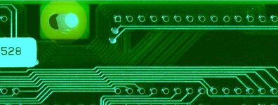
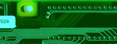
Still waiting for parts, so took a look at the BigROM Bus removal campaign.
1) can you identify what ROM packages fits and find a pinout link for me to run down?
2) figured I’d check traces that may or may not be necessary to keep.
1) Which ROM fits the footprint
I measured U25 and U26 in your component-side photo. Both are 40-pin DIP footprints with 0.6" row spacing, 20 pins per side on a 0.1" pitch. Pin 1 is the square pad at the notched end of each outline.
That fits the
16-bit-wide JEDEC EPROM family in a 40-pin package:
- 27C1024 (64K × 16)
- 27C2048 and 27C4096, which use the same 40-pin layout with more address lines
This also makes sense for the board. The SE's PDS bus is 16 bits wide, and one x16 part covers what the Hi/Lo pair (U19 + Ux) does with two 8-bit 27C256s. Two footprints would mean more capacity or alternate ROM options. That's my inference from the package, not something the board confirms.
To confirm it with your meter, check the power pins against the datasheet. Pin 40 should go to +5V, and the ground pins should buzz to GND. If they match, it's the x16 EPROM footprint.
Datasheet links for the pinout:
2) Which red traces can go
At this resolution I can't reliably call each red trace from the drawing. Sort them yourself with this rule. For each U25 or U26 pad that has a red trace, count how many
populated parts that net reaches: U19, Ux, the GALs, the VRAMs, or J3.
- 0 populated parts: delete the whole trace.
- 1 populated part: it's a stub. Delete the red run; the live pin keeps its other connections.
- 2 or more populated parts: the empty pad is working as a junction. Keep the net and route it directly between the live parts.
Two things I'd look at first:
- The long red runs under Ux and U19 toward the right edge. My guess is they head for J3 as data or address lines, which the live ROMs share. That means trimming the stub and keeping the net, not deleting the whole line.
- Every via on a red trace. A via can carry the net down to the inner layer, where it may connect to something live that you can't see.
If you mark each U25 or U26 pin with its buzz result using your Firm / Ratsnest / WTF? codes, I can go through the list and sort every trace into delete, trim, or reroute.
That was my line of thought, figuring that any buried traces heading inboard can be rerouted to the top layer on that broad highway.
- Any trace routed only between the BigROM thruholes creating a ROM pair bus can be tossed immediately?
- I’m guessing that the long traces between ROM area and BigROM bus may or may not be required?
1) Traces only between U25 and U26 pins: yes, toss them. Two x16 ROM footprints sharing address and data lines is exactly what you'd expect. Check one thing first: that no pin on that pair-bus also has a via or a trace leaving the pair. If every pad on the net belongs to U25 or U26, it's dead copper.
2) The long runs between the ROM area and the BigROM: it depends on how each net is chained. For each long trace, find where the U19/Ux pin gets that signal from.
- The ROM pin has its own route back to the source (J3 or a GAL): the long run only feeds the BigROM. Toss it.
- The ROM pin's only connection is that long run: the signal goes source → BigROM pad → long trace → ROM pin. The empty footprint is acting as a pass-through, so the trace is required. Route it straight from the source to the ROM pin on your top-layer highway.
The meter won't separate these cases, because both show continuity. Count the copper at the ROM pin instead: one trace leaving it means pass-through, two or more means the BigROM leg is only a branch. Also check each via for a branch running through the inner layer.
Chip-select and output-enable lines: if a GAL output drives only the BigROM's chip-select or output-enable, you can drop that trace too. The unused GAL output just floats, and the fuse map doesn't change.
Your plan to move the inner-layer traces up to the highway works. It also leaves the inner layer free to be a solid plane.
Thanks for the datasheet links, they come up empty, but now I’ve got part numbers to search. Figuring pinout overlay will help a lot.
Sorry the links came up empty. A few search terms that should turn up the 40-pin x16 datasheets:
- Am27C1024 (AMD)
- M27C1024 (ST)
- Intel 27C210, Intel's 64K × 16 part from the same period
The 27C2048 and 27C4096 datasheets use the same 40-pin layout. Either will do for your overlay.
When you place the overlay, find pin 1 at the square pad on the notched end of each footprint. Your drawing is rotated 180° from the photo, so pin 1 on U25 and U26 will land at the opposite corner from where it sits on the board.
Once you have a pinout diagram, send me a screenshot. I'll format it the way you like for pasting into Illustrator: left and right columns, pin number plus two spaces plus signal name, double-spaced.
Sounds great! The full board pics above are those you cleaned up for me. At that point the card was right side up and the ICs were upside down. Those pics were highest resolution and the easiest to locate.
Artwork is now IC notch upward, card upside down orientation. Here’s a better pic of the new traces. Data lines coded purple run through the resistor array and up the solder side to VRAM/Vias.
It looks like they branch from there to socketed ROM and U25. Expecting 14 more connections to appear across the South 40. WAG would be that the data bus runs (mostly on internal layer bus) to U26 in the North 40. Pinout overlay will tell.
This new orientation reads well. The numbers so far support your guess.
Sixteen data lines, everywhere:
- Resistors: there are two banks of 8, which makes 16. That fits series resistors on D0–D15 of the SE's 16-bit data bus, sitting between J3 and the rest of the board.
- VRAM: the D41264 is 64K × 4, so four chips give 16 I/O lines.
- Socketed ROMs: 8 data lines each. One of U19/Ux carries the high byte and the other the low byte, which makes 16.
- U25: a x16 EPROM would take all 16 data lines itself.
So your 2 found plus the 14 you expect gives exactly the full bus. If the pattern holds, every one of the 16 will reach the VRAM I/O, one ROM socket, and U25.
A quick test once the pinout overlay is in: if U25 is a 27C1024-family part, its 16 data pins should sit in two blocks of eight, split by a ground pin. That's roughly pins 3–10 and 12–19, but confirm against the datasheet. If your purple buzz hits land on those two blocks, you've identified the part. If U26 is a second x16 ROM, the same 16 lines will show up on the same pins there. Your guess that they travel north on the inner-layer bus would fit.
For the removal plan: the BigROM taps the data bus after the resistors. Cutting the U25/U26 branches leaves the resistor → VRAM and resistor → ROM paths untouched, provided each ROM pin still has its own route back to the resistors. It's the same pass-through check as before: if the only route to a ROM data pin runs through a U25 pad, that leg has to be rerouted.
Send the pinout diagram when you find it, and I'll format it for your overlay.
Here it is.
I've formatted the 27C1024 pinout for your overlay in 27C1024-Pinout-U25-U26.txt. It's split into left and right columns in physical DIP order (1–20 down the left, 40–21 down the right). Each entry is the pin number, two spaces, then the signal name, double-spaced. Active-low signals keep the datasheet's # suffix (CE#, OE#, PGM#), so no overline character has to survive the paste.
Once it's placed, check these on U25 and U26:
- Data bus: your purple buzz hits should land on pins 3–10 (DQ15–DQ8) and 12–19 (DQ7–DQ0), with ground on pin 11 in between. If they do, the footprints are confirmed as x16 ROMs.
- Power pins: pins 11 and 30 should buzz to GND, and pin 40 to +5V.
- Pin 1 (VPP): in read mode this is usually tied to +5V or straight to VCC. That's another quick power check.
- CE# (pin 2) and OE# (pin 20): trace these back to find which GAL outputs drive the BigROM. Those traces can go in the clone.
- A0–A15: these probably share address lines with the socketed ROMs. Apply the pass-through check to each one before you cut anything.
Thanks, back to AI playtime!
Have fun, jt. Send the overlay over when the buzz hits are on it.
____________________________________________________________
FPD
Picking the FPD clone back up. Here's where things stand:
- Pinout verification is done and picture-locked (.035/.036), including the U6/U7 SN74LS393 fix and U10 confirmed as a GAL16V8.
- Component-side buzz-testing is underway on the two-file .036+ workflow. The latest was .039, which added the confidence-coded trace legend and got most of U22 and its VIAs buzzed.
- Hardware for testing is mostly in hand: the clean MagicBus adapter came in at $35, the BlueSCSI is ordered with the multi-boot SD layout planned, and the cutaway SE is waiting on a few parts. Both cards need to pass a proof-of-life test through the Extron before any desoldering.
- Parked for later: the North 40/South 40 FPGA split, GAL fuse readout through your friend, and the rotation transform, which is already spec'd.
What are you picking up today? It could be a new .04x buzz file to cross-check, the BlueSCSI image setup, card testing, or something else. If you've got files to share, attaching them works fine. I can also connect to your FPD project folder on the ProBook if that's easier.
Rummaged through the project parts/prototyping drawer and I’ve got much of what I need on hand:
-Solder Cup HD-15M for cable build to plug into the back of the Extron Scaler
- EPT103-4-174 2172 DIN96M RA Wire Wrap Connector for PDS Adapter
- Single Row .1” pitch Wire Wrap Headers and tall Sockets to match
Unfortunately, the double row Zig-Zag thruholes for J38 are more than .1” apart, so I can’t use a .05” Perf Board, a custom PCB will be required. In that case I don’t necessarily need wire wrap capability. Patch wires will work if a couple of connections are off. But if routing the traces proves as tight as I think it will, I can go with the wire wrap components and only wrap a row or two at the top if required.
Looks like it’s time to look at some KiCAD videos. You can provide me with the schematic for the SE PDS to J38 thruholes adapter board from the files we have, no?
Not from anything I can see this session, jt. None of the earlier uploads carried over. The 68kMLA PDS-to-MagicBus pinout, the Component-Side-Test PDFs and the board photos all lived in earlier chats. No folder on the ProBook is connected yet either. I only have my notes, and they record that the pinout exists but not what's in it. I'm not going to rebuild a 60-line netlist from memory. One swapped address line and you'd lose an evening chasing a problem that's really in the adapter.
Here's what I need to draw it properly:
- The PDS-to-MagicBus pinout from that 68kMLA post, as a screenshot or copy/paste. I can't reach 68kmla.org from here.
- Which board J38 is on. I'm assuming J38 is the staggered 60-position footprint that mates with the FPD's JAE PICL-60P-LT, on the MagicBus card side. If it's the Radius16's designator or something else, tell me.
- J38 footprint dimensions, taken with calipers from the clean MagicBus card: pin pitch along each row, spacing between the two rows, stagger offset, and hole diameter. You can also send the JAE datasheet if you can find one. A custom footprint needs real numbers, and I'd rather have your measurements than a guess.
Tip: you now have the clean MagicBus card, and that's a better source than the forum post. Buzzing its DIN96 pins to its J38 holes gives you the actual connection map. I can cross-check that against the 68kMLA pinout, and any row where they disagree gets flagged before it goes into copper.
Once I have those, I'll build:
- A KiCad schematic (.kicad_sch) with a DIN 41612 96-pin symbol, a custom 60-pin staggered symbol for J38, and the net connections between them. Unused DIN96 pins get no-connect flags.
- A matching netlist table (CSV or your double-spaced Illustrator format) so you can check it against your AI9 artwork.
- A custom J38 footprint built from your measurements, so the PCB layout starts with the right hole pattern.
Two questions to settle before layout. Neither blocks the schematic:
- Your DIN96M should mate with the SE's PDS connector, but check the gender against the logic board.
- The right-angle part means the adapter board stands vertical. Which side J38 lands on decides whether the FPD card faces outboard, as in your prototype orientation plan.
MagicBus Card arrived in good order, do these pics help?
Yes, they help a lot, jt. The photos settle what the board is and roughly what the connector footprint looks like. They aren't enough for the actual pin-to-pin map.
Name correction first. The silkscreen that reads "J38" is actually
J3B, the middle row of
J3. J3 is the 96-pin DIN connector (rows J3A, J3B and J3C, pins 1–32). The staggered double-row footprint is
J2, the black JAE 60-pin connector (rows J2A and J2B, pins 1–30). I'll use J2 and J3 in the schematic so it matches the real board.
What the photos show:
- Two-layer board, simple wiring. On the dark side, each DIN pin runs up to a pad in that staircase pattern. On the green side, a trace runs from that pad straight across to the J2 footprint. There's no logic on the board, only wiring, plus a few power runs along the lower right and one strap-like link near J2. So your adapter really is a MagicBus clone with different connectors.
- J2 pitch, measured from the photo. The DIN connector's standard 2.54 mm pitch gives me a scale for the photo. On that scale, J2's contacts are about 1.27 mm (0.050") apart along each row. The legs fan out into four offset columns of holes, about 6 mm wide overall and about 38 mm long. That fan-out is why the spacing didn't match any perfboard grid. Treat these as a sanity check only: take the final numbers from calipers.
- The dark-side photo is mirrored. The silkscreen reads backwards, so it looks like your usual reversed reference view. I'll keep that in mind for any pin I read from it.
Why I won't pull the netlist from the photos. Matching 60 pads in the staircase back to the right column out of 32 DIN positions, at this resolution, is too error-prone. Buzzing it takes about 60 quick meter checks on a board this simple. It can also catch power pins that connect to more than one place, which the photos can't show.
Check the connector gender. The MagicBus's DIN connector looks like the
female receptacle, which would mean the SE logic board has the male pins. If so, the DIN96M right-angle part you pulled from the drawer won't plug into the SE's PDS slot. It might still suit the FPGA board plan. Worth confirming against the logic board before layout.
Next step: buzz each J2 pin (1A–30A, 1B–30B) to its J3 pin (row letter plus number), and mark any J2 pin that connects to more than one J3 pin, since those are likely power or ground. Add the 68kMLA pinout and caliper measurements when you have them. I'll then build the KiCad schematic, the netlist table and the J2 footprint, and flag anywhere your buzz results and the forum pinout disagree.
I can also make you a blank buzz sheet with J2 on the left and blanks for the J3 pin and notes, in your double-spaced paste format or as a spreadsheet.
Getting a little ahead of me, mostly updating you on hardware progress today:
Completed steps:
- tested DIN M RA wire wrap connector in PDS slot. Beautiful, WW pins point outward.
- SE Logic Board has been removed from the clear case
- now mounted to a plexi carrier and moved to my open SE/30 test stand setup
- SE powers up and searches for a boot disk
- Cable extension works great!
- BlueSCSI is mounted via the slide in HDD carrier setup mounted to the PSU
- tested SE/MagicBus/FPD and it boots to questioning Floppy, so good to go.
Next steps:
- build a speaker cable extension
- build HD-15 to J1 Cable for Extron connections
- image System 6.0.8 on SD card for boot disk in BlueSCSI
Nice progress, jt. The flashing question-mark floppy on that screen means the SE, MagicBus and FPD all run together without a crash, and that's a real milestone.
Correction: you've now shown the DIN96M right-angle part seats in the PDS slot, so my gender warning was wrong. Better still, it means the FPGA prototype's vertical-mount plan works with the connector you already have.
Some notes on the next steps:
HD-15 to J1 cable for the Extron:
- Don't forget J1 pin 6, the sense line. It has to be tied to ground inside the cable. Otherwise the card's video drivers shut down at startup and you'll get nothing, which looks like a dead card.
- Suggested wiring, using standard VGA pin numbers on the HD-15:
| J1 pin | Signal | HD-15 pin |
|---|
| 2 | Ground | 5, 6, 7, 8, 10 |
| 3 | Video | 1, 2, 3 (red, green, blue) |
| 6 | Sense | Tie to ground |
| 7 | H sync | 13 |
| 9 | V sync | 14 |
- Optional: a series resistor on the video line. The Extron's color inputs expect about 0.7 V, and 5 V TTL overdrives them. That's harmless for a proof-of-life check, but it may have caused some of the beat pattern you saw with the TPD. A resistor of roughly 470 Ω in series with each color pin brings the level down, and it's easy to add in the solder-cup shell. The Extron's sync inputs accept 2.75–5 V, so TTL sync connects directly.
System 6.0.8 image on the BlueSCSI: the file name sets the SCSI ID. Name it HD10_512.hda to put it on ID1, matching your ID scheme (the "1" is the SCSI ID and the "0" is the LUN). It also fits your plan to add 7.0.1 and the others later.
Send the J2-to-J3 buzz results whenever you get to them, and I'll start the adapter schematic.
____
That's useful, and it might shorten the path to a proof-of-life test.
- Boot from a floppy first. A System 6.0.8 boot disk (the System Tools disk, or any bootable 800K disk) gets you to a desktop without waiting on the BlueSCSI image. Once the Mac reaches the desktop, the FPD's drivers in the declaration ROM should load. That's enough to try the J1-to-Extron cable as soon as it's built.
- Use it as a second drive. You can use it with the SE's internal drive if one is still hooked up through your cable extension. Two drives make disk-to-disk copying and installing from floppies much less of a swap-fest.
- It plugs into the SE's DB-19 external floppy port. Every SE logic board supports 800K, whether it's the original 800K model or the later SuperDrive (FDHD) version.
The BlueSCSI image can come later, once the card has shown it's alive.
It would be if I had 6.0.8 install set on floppy. :-/
You probably don't need floppies at all. The BlueSCSI gives you a faster route.
- Use a ready-made hard disk image (easiest). Prebuilt, bootable System 6.0.8 hard disk images are widely shared, including on Macintosh Garden, where you got the ROM dumps. Copy one onto the SD card, rename it HD10_512.hda, and the SE should boot from it straight away, with nothing to install. You'd then have a desktop for the FPD test with no floppies involved.
- Write floppies on another vintage Mac. If one of your fleet has a SuperDrive, Disk Copy 4.2 can write 800K disks from install-set images. That's more work than the option above, for the same end result.
- Your PC's floppy drive won't work on its own. Mac 800K disks use a different recording format that ordinary PC drives can't write. Flux-level tools like Greaseweazle or FluxEngine can do it with a PC drive, but that means buying hardware you don't need, given the BlueSCSI.
A clean install from the install disks can wait for the multi-partition image you're planning. For proof of life, any image that boots will do.
Nice bit of information on the Extron’s input requirements, thanks. I hadn’t forgotten the sense line. Thanks much for giving me the cable pinout. I’ve got a nice box of assorted resistors ready and waiting for both applications.
The SE/30 test rig I pulled down off the shelf keeps my hands farther away from the zappy parts. May or may not fab a plexi shield, dunno, I’ve worked with them live many times in the past.
Good plan. A few tips for the BigROM buzz:
- Pull the socketed ROMs and GALs first. Otherwise the meter can read through a chip's internal protection diodes and show connections that aren't really there.
- Watch for through-routes. Some traces may just pass through a BigROM hole on their way to another part. Those are the nets to keep, rerouted onto the top layer, rather than removing them with the rest of the bus.
- Check each hole against the U19 and Ux socket pins. The bus most likely just duplicates the installed ROMs' address and data lines. If a hole matches a socket pin, that confirms it; if one doesn't, it needs a closer look.
- Test each hole against both inner planes. A hole that beeps to ground or 5 V is a power pin, not a bus line, and it helps confirm which plane is which.
Log each hole and whatever it beeps to. When you send the results, I can sort them into three piles: safe to delete, needs rerouting, and power.
Done.
Nice work, jt. Nothing came through with that message, though. Send the buzz log however it's easiest: a photo of your notes, an AI9/PDF export, or a typed list. I'll sort it into safe to delete, needs rerouting, and power.
Copy.
Ready when you are.