Apple TechStep Replacement ROMs, cartridges, software, and more!
- Thread starter jajan547
- Start date
You are using an out of date browser. It may not display this or other websites correctly.
You should upgrade or use an alternative browser.
You should upgrade or use an alternative browser.
Thank you for the clarifications. Basically, one should not use an Assembly service because in order to use that programmer, you would need to socket the ROM chip, program it, then solder it in. In other words, one should do the soldering assembly themselves. I don't see that as a big issue because the component count is low.Both .stls will work I've printed both. As for your question about the revised bin this was for CPU tests vol4, the revised is the correct one and the other is a messed up prototype ROM image. I found that the chips listed all work well in programming using a mini Pro (link here). When it comes to the revision 1 and 2 boards there were different board revisions CPU tests 1 & 2 as well as SCSI HDD tests used the REV 1 (cart 1) board and the CPU tests 3 and 4 used the REV 2 (cart 4) board. I believe both bin files for CPU tests vol 2 to each work just fine so that's pick and choose. Regarding your question about PCB ordering I think it's an issue on their end because I used JLCPCB and was able to see and order my boards just fine. Last thing I want to note is there are two separate versions for each revision one is surface mounted components the other is dip based components. I'm also not sure why that link is in there but like I said with JLCPCB I had no issues.
Just to clarify, I am not trying to be critical. In am simply thinking how to hand-hold newbies to get from point A to point B. Newbies may come along and find this thread, then want to know how to easily build a cartridge. So I was thinking of a step-by-step approach to aid them in achieving that.
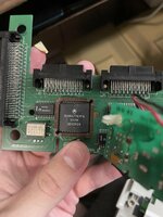
correct, I would recommend using a 32pin plcc socket when you assemble this but as such I made some without the socket. I have attached pictures of both the case and a cart 4 board with SMD components with a CPU Tests vol.4 ROM image. And no worries I completely understand and appreciate feedback. Image link is HEREThank you for the clarifications. Basically, one should not use an Assembly service because in order to use that programmer, you would need to socket the ROM chip, program it, then solder it in. In other words, one should do the soldering assembly themselves. I don't see that as a big issue because the component count is low.
Just to let everyone know (even though it's written in the Parts List RTF file, the connector shown in your photo is in stock on Mouser right now ($2.90 for 1pc, shipping extra).correct, I would recommend using a 32pin plcc socket when you assemble this but as such I made some without the socket. I have attached pictures of both the case and a cart 4 board with SMD components with a CPU Tests vol.4 ROM image. And no worries I completely understand and appreciate feedback. Image link is HERE
Also on digikey, I apologize for the bad lighting I’ll take better ones later.Just to let everyone know (even though it's written in the Parts List RTF file, the connector shown in your photo is in stock on Mouser right now ($2.90 for 1pc, shipping extra).
View attachment 5086
Okay I went through and simplified some things. I even added some instructions and a new images folder. Hope this is better and helps people out.
******edit I added this folder to the first page top post******
******edit I added this folder to the first page top post******
Attachments
Last edited:
What's the link to the digikey page? I did a search for the part number FCN-215Q040-G/0 but it didn't find anything useful.Also on digikey, I apologize for the bad lighting I’ll take better ones later.
I assume DigiKey dropped it but mouser has it.What's the link to the digikey page? I did a search for the part number FCN-215Q040-G/0 but it didn't find anything useful.
How many of you own a TechStep or want to buy one some day?
*Hand up high in the air* Me wanna buy one!

This project is also discussed in this Thread 'Recreateing the Apple TechStep'.
Last edited:
Indeed it is Max and I are currently working on that.*Hand up high in the air* Me wanna buy one!
This project is also discussed in this Thread 'Recreateing the Apple TechStep'.
Also fun fact the TechStep has a FPU it is a Motorola 68882.
Hi @jajan547!

Can you remove that yellow sticker off the chip in the socket? That will help to make sure what it is.
I do not think it is a 68882 FPU because the Motorola part number for that begins with MC. The chip with the yellow sticker has a part number starting with XC.
Last edited:
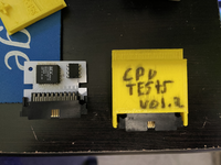
Oh we found that already here's a picture of what it really is though.Hi @jajan547!
Can you remove that yellow sticker off the chip in the socket? That will help to make sure what it is.
Attachments
Oh we found that already here's a picture of what it really is though.
Aha! That is a Motorola 8-bit microcontroller (MCU). Here are the details. It may differ since TechStep was back in the 1990s.
Introduction
This document contains a detailed description of the M68HC11 E series of 8-bit microcontroller units
(MCUs). These MCUs all combine the M68HC11 central processor unit (CPU) with high-performance,
on-chip peripherals.
The E series is comprised of many devices with various configurations of:
• Random-access memory (RAM)
• Read-only memory (ROM)
• Erasable programmable read-only memory (EPROM)
• Electrically erasable programmable read-only memory (EEPROM)
• Several low-voltage devices are also available.
With the exception of a few minor differences, the operation of all E-series MCUs is identical. A fully static
design and high-density complementary metal-oxide semiconductor (HCMOS) fabrication process allow
the E-series devices to operate at frequencies from 3 MHz to dc with very low power consumption.
Features
Features of the E-series devices include:
• M68HC11 CPU
• Power-saving stop and wait modes
• Low-voltage devices available (3.0–5.5 Vdc)
• 0, 256, 512, or 768 bytes of on-chip RAM, data retained during standby
• 0, 12, or 20 Kbytes of on-chip ROM or EPROM
• 0, 512, or 2048 bytes of on-chip EEPROM with block protect for security
• 2048 bytes of EEPROM with selectable base address in the MC68HC811E2
• Asynchronous non-return-to-zero (NRZ) serial communications interface (SCI)
• Additional baud rates available on MC68HC(7)11E20
• Synchronous serial peripheral interface (SPI)
• 8-channel, 8-bit analog-to-digital (A/D) converter
• 16-bit timer system:
– Three input capture (IC) channels
– Four output compare (OC) channels
– One additional channel, selectable as fourth IC or fifth OC
• 8-bit pulse accumulator
• Real-time interrupt circuit
• Computer operating properly (COP) watchdog system
• 38 general-purpose input/output (I/O) pins:
– 16 bidirectional I/O pins
– 11 input-only pins
– 11 output-only pins
• Several packaging options:
– 52-pin plastic-leaded chip carrier (PLCC)
– 52-pin windowed ceramic leaded chip carrier (CLCC)
– 52-pin plastic thin quad flat pack, 10 mm x 10 mm (TQFP)
– 64-pin quad flat pack (QFP)
– 48-pin plastic dual in-line package (DIP), MC68HC811E2 only
– 56-pin plastic shrink dual in-line package, .070-inch lead spacing (SDIP)

Last edited:
Cool!Added a better photo of what a finished board and case look like.
Only need those two chips and the cartridge? Does that connect somewhere else? 
Connects to a TechStep because the Techstep's need these packs to troubleshoot certain computers. @max1zzz and I are working on a new TechStep but for those of you who own one and want to make any ROM you need that's what this is all about.Cool!