Yes the FPU is the yellow labeled chip. I might be able to do a ROM dump.No, the HM62256 is a 32kB static RAM.
Is the FPU the yellow labelled chip? Possibly it asks the logic board to do calculations and compares them to what this one gives.
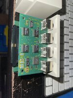
The 68HC24FN is an evolution of the HC05 uC used as EGRET, likely one is wired to the sram and cartridges. Maybe it's possible to dump their ROM, not sure. There's also a registered PAL to dump…
Apple TechStep Replacement ROMs, cartridges, software, and more!
- Thread starter jajan547
- Start date
You are using an out of date browser. It may not display this or other websites correctly.
You should upgrade or use an alternative browser.
You should upgrade or use an alternative browser.
Also was wrong about the 68882, I’ll have to take it apart again and see what’s actually under the yellow.
Correction: The 68HC24 chips are called "Port replacement unit", which I suppose are the 68HC11 equivalent of a VIA or PIA, some kind of port extender to replace the pins of the uC when it's used with an external memory.
Yeah it's much smaller (52pins) than an FPU. I'd say it's a 68HC11 of some sort, since the other chips aren't uC.Also was wrong about the 68882, I’ll have to take it apart again and see what’s actually under the yellow.
I also forgot to take apart the port pack I’ll do all of this later tonight.Correction: The 68HC24 chips are called "Port replacement unit", which I suppose are the 68HC11 equivalent of a VIA or PIA, some kind of port extender to replace the pins of the uC when it's used with an external memory.
Yeah it's much smaller (52pins) than an FPU. I'd say it's a 68HC11 of some sort, since the other chips aren't uC.
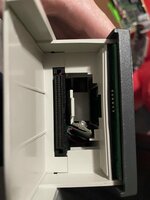
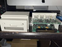
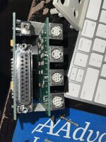
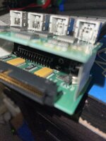
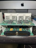
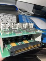
Here are photos of the Port PackConnector seem to be similar to the SCSI LVD connector but with 80 & 40 pins…
Attachments
-
 59EDA9E6-BB7D-4E91-A9BD-EFF72F5C5913.jpeg1.2 MB · Views: 270
 -
 952EDF75-0E3C-44F8-AAC0-493B3C4D9DA2.jpeg1.5 MB · Views: 289
 -
 08E63989-24AA-4ACA-B5FC-9ED9E32AED52.jpeg1.8 MB · Views: 402
 -
 6C6ED355-BEE3-411C-BA4C-E70EB13F944B.jpeg1.8 MB · Views: 246
 -
 F7C92685-5C59-4E75-8F13-2DFD31E1E44F.jpeg1.9 MB · Views: 277
 -
 BC4F9A66-834A-4DC9-95CC-CD1F0E067F03.jpeg1.5 MB · Views: 267
 -
 0B385499-9771-442F-839D-758DFDECB39F.jpeg1.3 MB · Views: 383
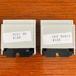
Somehow, I have managed to accumulate three TechSteps over the years, but only a small assortment of different ROM cartridges.How many of you own a TechStep or want to buy one some day?
- CPU Tests Vol. 1, v. 1.1.1 (x3)
- SCSI HD Tests, v. 1.0 (x2)
- CPU Tests #188
- SCSI HD #188
Attachments

THose are prototype ROMs and they are pretty much the same as the released ones, mind uploading them?Somehow, I have managed to accumulate three TechSteps over the years, but only a small assortment of different ROM cartridges.
However, I also have a pair of ROMs with simple typewritten labels:
- CPU Tests Vol. 1, v. 1.1.1 (x3)
- SCSI HD Tests, v. 1.0 (x2)
Has anyone seen cartridges labelled like this?
- CPU Tests #188
- SCSI HD #188
Either the chip will be an MX1000QC-12 or a AM27C512 you will need to dissassemble the rom pack (just unclips or pops apart) from here you need a 32 pin PLCC adapter and a tl866 (link here). Once the ROM pack is open pop out that chip that is socketed it will be the ROM.Sure, I can upload them … what the best way to do that? Are there instructions posted?
Probably can, it’s just you have to pry plastic and it gets a bit scary there but I’ll give it a shot tonight.@jajan547 don't suppose you got some pics of the LCD? Mine is very dim and when I dig it out of storage I'd like to replace the 1602 if I can.
I don’t mind, no worries I am looking for units outside of the USA, so if you have an extra let me know.Ah don't worry - I'll sort it when I need to. Don't want you to damage yours on my behalf!!
Hey there if you trust me I'll cover shipping both ways to get the ROMs from these and then send them back.Ok, I’ll look into that.
That’s a good idea, actually.Hey there if you trust me I'll cover shipping both ways to get the ROMs from these and then send them back.
We’ll figure this out in DMs.
Hello this is a crosspost from another site (68kmla), We know that the TechStep was a short lived but very useful tool and it can test many components and issues on these Old Macs. A team of three people have made all of this possible. Below you will find a .zip file containing all of the resources, build guides, documentation, .stl files for the 3D printable cases, as well as the ROM images and boards themselves. Each category has been broken down into folders for your use, enjoy!
Creators of this project are @jajan547, @Elemenoh, and @SuperSVGA
Before I begin, I just wish to express my sincere amazement and appreciate of this amazing project. The work that went into making this a reality is simply astounding!
I now have some questions and comments about the contents of the attachment in the opening post:
Let's go about this assuming that folks who find this thread and who are interested in building themselves a ROM pack have zero experience making PCBs, programming chips, etc.
QUESTIONS/COMMENTS:
1. What are the differences between TechStep Cartridge Rev1 & Rev2? (The fact both are included implies both may be needed, depending on the use case.)
2. There are two "Cart1" and two "Cart4" files with one of each having "M95020" in the name with no explanation, and without viewing the Gerber files, it's impossible to know which is which. However, from what I can see, the M95020 version uses all SMD components, while the other version uses a DIP version chip for U2. Even so, when I load each file into the PCBWay interface, only the M95020 version looks right, as shown below. The other Gerber has some serious problems. Could that be a problem with PCBWay's Gerber viewer or that Gerber file?
The Gerber file without M95020 in the name:
3. Inside each of the Gerber ZIP files, there's a text file that says this...
Clicking that link leads to this web page:

It's a little confusing because it says in step 1...
- Finish the schematic and PCB design at EasyEDA.
One is then left to wonder: "schematic? what schematic? and how do I finished it?"
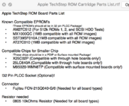
I do see this "BOM" of sorts in your archive (opening post attachment)...
But it doesn't list specifics like quantity, resistor tolerance (i.e., does the factory cartridge use 5% tolerance?), and which cartridge name applies to which parts.
I am going about this as a newbie. If a newbie has the goal of making Cartridge 4, for example, they would need to do this:
1. Figure out which Gerber to use, then choose a PCB maker (like PCBWay or JLCPBC) and upload it, then have them build it. Even though it is often said JLCPCB is cheaper than PCBWay, fact is that some folks who've been using PCBWay may wish to stick with them. So knowing how to accomplish PCB creation on PCBWay too may be helpful to some.
2. Figure out which parts one needs to order and what quantity (including the connector), and then determine if the PCB supplier (e.g., PCBWay) can build the board with those parts. PCBWay seems to have an Assembly service and they appear to be able to source parts too. Using their web interface, it seems they Assembly fee would come to US$30, which doesn't include the price of the parts.
3. Upload the STL files for the plastic case to a place that can build the case. PCBWay offers a 3D service, and their build using Resin would cost about US$25 for the 2 required pieces (not including shipping):
4. Figure out what is needed to program the "REVISED" BIN file to the ROM chip, and whether that can be done if one orders an "assembled" PCB from a place like PCBWay. (In other words, what programmer is required, and how does one interface that to the ROM chip for programming, and what software is required?)
5. One then needs to print the labels (contained as PDFs in the attachment in the opening post), and affix them to the 3D printed plastic case.
So any thoughts you can share on the above would be helpful to those wishing to create a finished cartridge, using the files attached to the opening post.
Thanks!
Attachments
Both .stls will work I've printed both. As for your question about the revised bin this was for CPU tests vol4, the revised is the correct one and the other is a messed up prototype ROM image. I found that the chips listed all work well in programming using a mini Pro (link here). When it comes to the revision 1 and 2 boards there were different board revisions CPU tests 1 & 2 as well as SCSI HDD tests used the REV 1 (cart 1) board and the CPU tests 3 and 4 used the REV 2 (cart 4) board. I believe both bin files for CPU tests vol 2 to each work just fine so that's pick and choose. Regarding your question about PCB ordering I think it's an issue on their end because I used JLCPCB and was able to see and order my boards just fine. Last thing I want to note is there are two separate versions for each revision one is surface mounted components the other is dip based components. I'm also not sure why that link is in there but like I said with JLCPCB I had no issues.