Community project? NuBus-to-SPI interface... aiming toward ESP32-based WiFi card

Zane Kaminski

Administrator
Staff member
Founder
Sep 5, 2021
372
610
93
Columbus, Ohio, USA
The accelerator I posted about yesterday is a bit advanced so I figured I'd finally do a schematic for an idea I've had for a while. This one is more softwarey and there are a lot of great software developers out there so hopefully we can get some kind of collaboration going.

One of the things complicating the connection of new peripherals (e.g. ESP32-based WiFi modules) to old systems is the parallel vs. serial bus distinction. Old systems use parallel buses with tens of pins. New microcontrollers don't have so many pins and instead are designed to use serial interfaces (e.g. SPI, I2C) to transfer data. Moreover, new microcontrollers and old systems alike work better in an interfacing application as the bus master. To work a peripheral, the Mac wants to, in the course of executing the relevant driver, write to some I/O registers to accomplish the desired function. The story is the same with an MCU. It doesn't work so well as an SPI slave. It works best when the MCU is the initiator of the SPI transaction. Some chips don't even support hardware SPI slave, or they might only support a slower data rate as a slave device, for example.

So here's the schematic design for a gizmo that allows a NuBus Mac to transfer data back and forth from any arbitrary device that can function as an SPI master. ESP32 is one of my favorite MCUs and you can immediately imagine a lot of applications enabled by just a low-to-medium data rate connection from the Mac to an ESP32-based module... WiFi networking, microSD storage, etc. The list goes on.

Now for the technical explanation of how this system is supposed to work. First I guess it would be instructive to look at a very simplified block diagram:
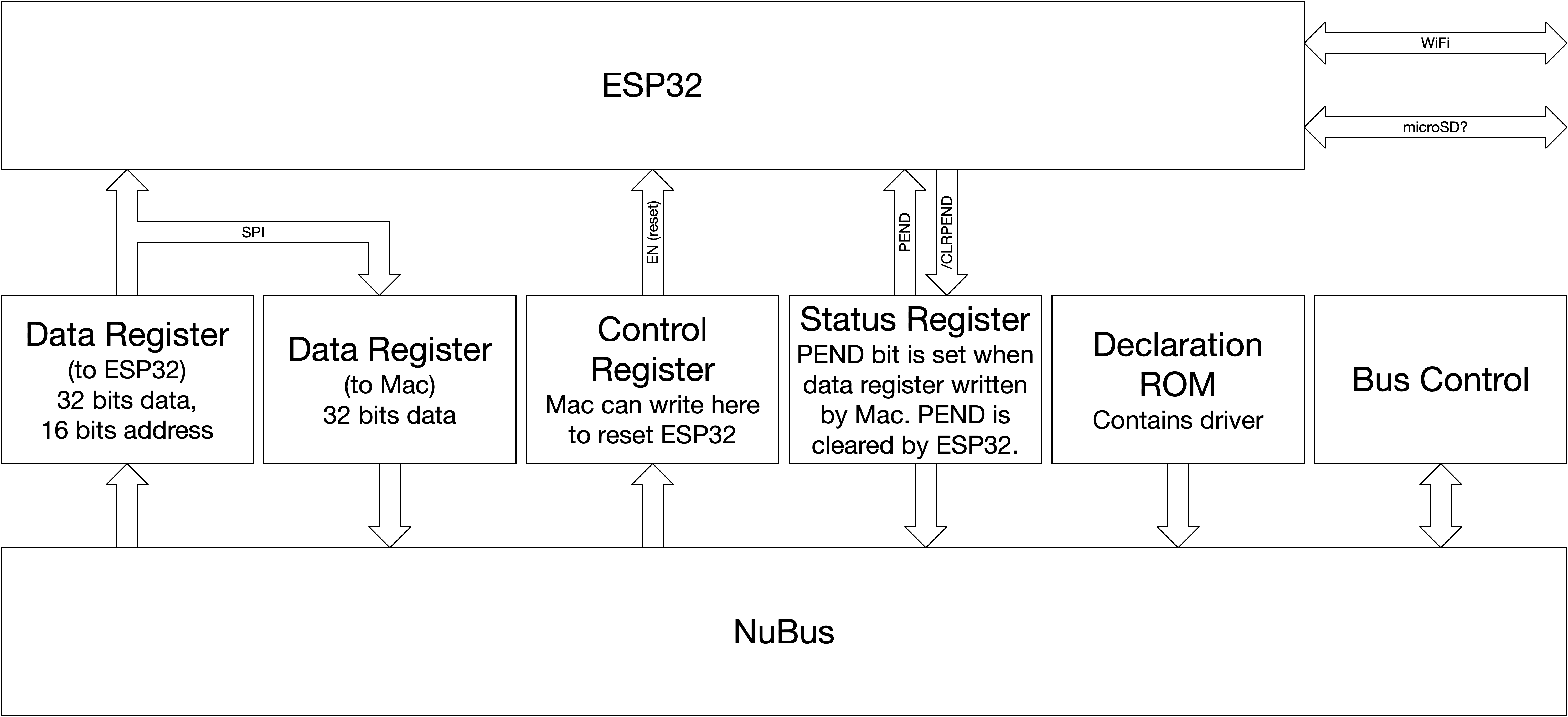
Architecture.png

There are a few blocks here and I'll explain the functions.

Let's get "Declaration ROM" out of the way... it's the flash that holds the declaration ROM driver that the Slot Manager looks for at boot to recognize a card. This allows us to install a driver in the machine before anything is even loaded from disk so we can implement bootable storage.

The key parts here are the two "Data Registers" and the "Status Register." The data registers are both shift registers. The Mac can write a 32-bit quantity into the card and the data is stored in the "Data Register (to ESP32)" for retrieval by the ESP32 along with a 8 bits of address and size information. Whenever the data register is written by the Mac, the PENDING bit is set in the status register. The PENDING signal is directly hooked up to the ESP32 so that it can receive an interrupt when new data has been written into the data register. When this happens, software on the ESP32 starts an SPI transaction and reads serially from the shift register the 40 bits placed by the Mac in the data register. Software on the ESP32 can interpret the data read as a command, block transfer data, whatever. Completely flexible. Once the program on the ESP32 is done processing the data from the Mac, if a response back to the Mac is required, the ESP32 can start another SPI transaction and load 32 bits of response data into the "Data Register (from ESP32)." Then once all processing of the command is complete, ESP32 asserts the /CLRPEND (clear pending) signal and the PENDING bit is cleared. While this is all occurring, the Mac busywaits for PENDING to be cleared. Once the Mac sees PENDING low it can read ESP32's response and send more commands/data to the ESP32.

"Control Register" is simple, just a 1-bit port that allows the Mac to toggle ESP32's reset signal. "Bus Control" implements the timing and select signals and whatnot required for the card to act as a NuBus slave and transfer data between the Mac correctly.

On to how to implement this...

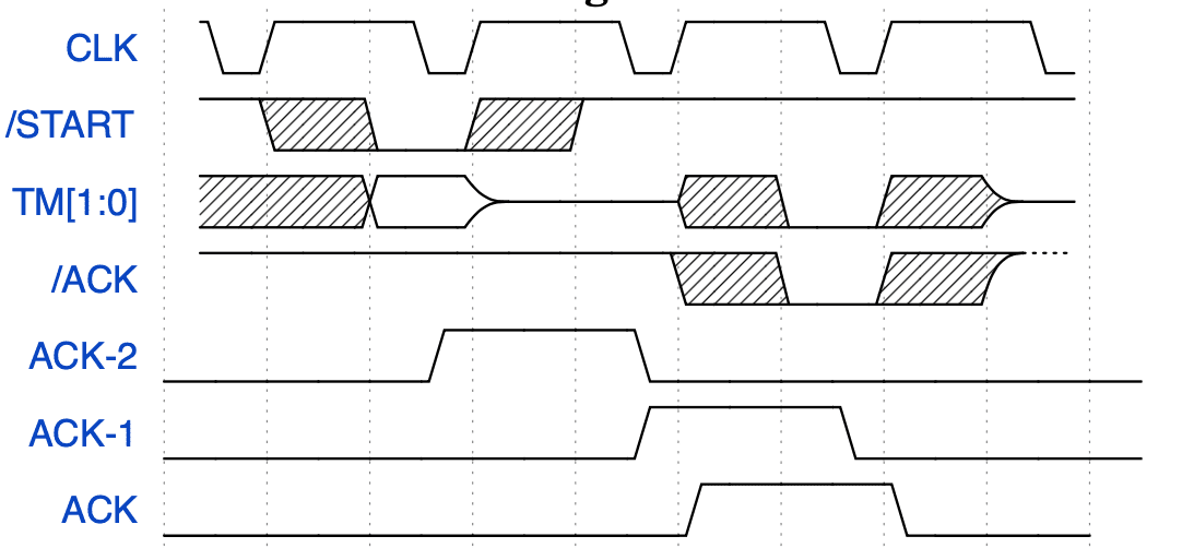
Here's the desired timing for the cycle termination aspect of the NuBus slave port:
Screen Shot 2021-11-03 at 7.55.40 AM.png

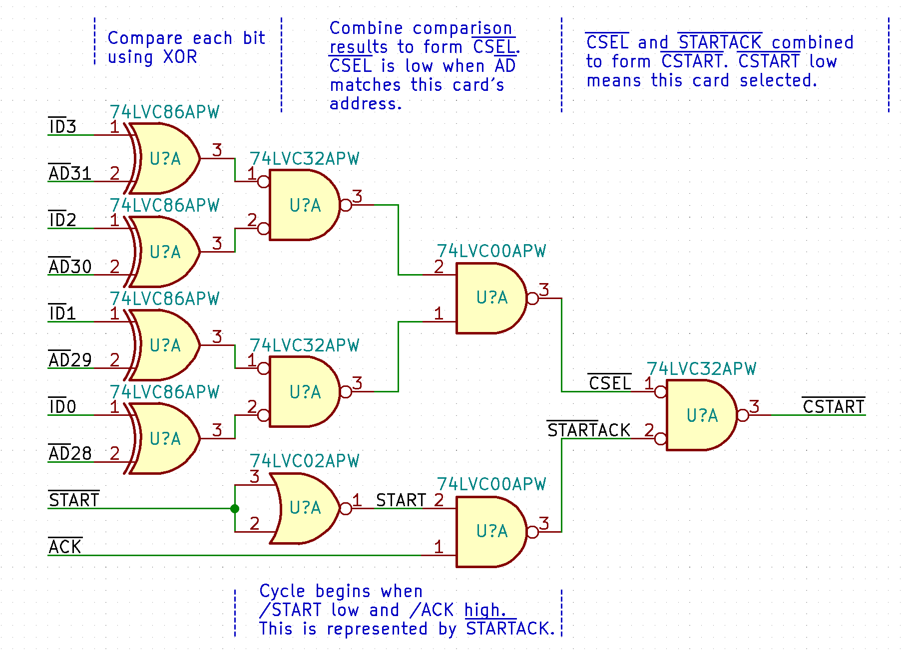
When /START is low, /ACK is high, and the upper bits of the address bus (not shown) match the hard-wired card ID pins on the NuBus connector, our card is considered to have been selected for a read/write transaction. We want to bring /TM[1:0] and /ACK low in response in order to terminate the bus cycle.
There is a complication of NuBus (actually it's helpful). All signals are read on the falling edge of CLK and change on the rising edge of CLK. The clock runs at 10 MHz (100 ns cycle time) and has a funky 75% duty cycle (high for 75 ns, low for 25 ns) in order to maximize the time after the rising edge before falling edge at which the signals are registered by the units on the bus. To detect a bus cycle aimed at our card, first we generate a signal called /CSEL which indicates that our card is selected on the bus. This is combined with /START and /ACK to get /CSTART. /CSTART is considered valid at falling edges of the clock and is low when the current card is being selected. /CSTART is registered at every falling edge, yielding the ACK-2 ("ACK minus two") signal. Then ACK-2 is registered at the next falling edge to get ACK-1, which is then registered at the next rising edge to get ACK-0. ACK-0 is inverted and goes directly to the /OE of the buffer that drives /ACK and /TM[1:0] low on the NuBus.

Here we have the schematic for generating the /CSTART signal:
Screen Shot 2021-11-03 at 8.08.21 AM.png


And here we /CSEL several times in a row to get ACK-2, ACK-1, and ACK-0. At the end of the register chain is a '125 buffer that outputs the correct cycle termination signals:
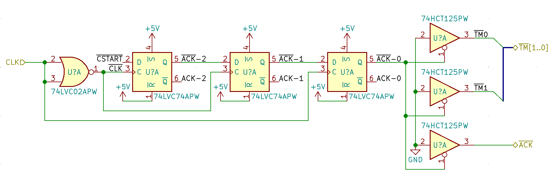
Screen Shot 2021-11-03 at 8.10.52 AM.png


Since NuBus is a multiplexed address/data bus, the address and transfer mode (read/write/size) are only available in the first clock cycle of the bus transaction. We have to register them so that we can use them later for ROM access and to load into the shift register going to the ESP32. We call the clock for the address/TM register ACLK. Here's the timing we want:
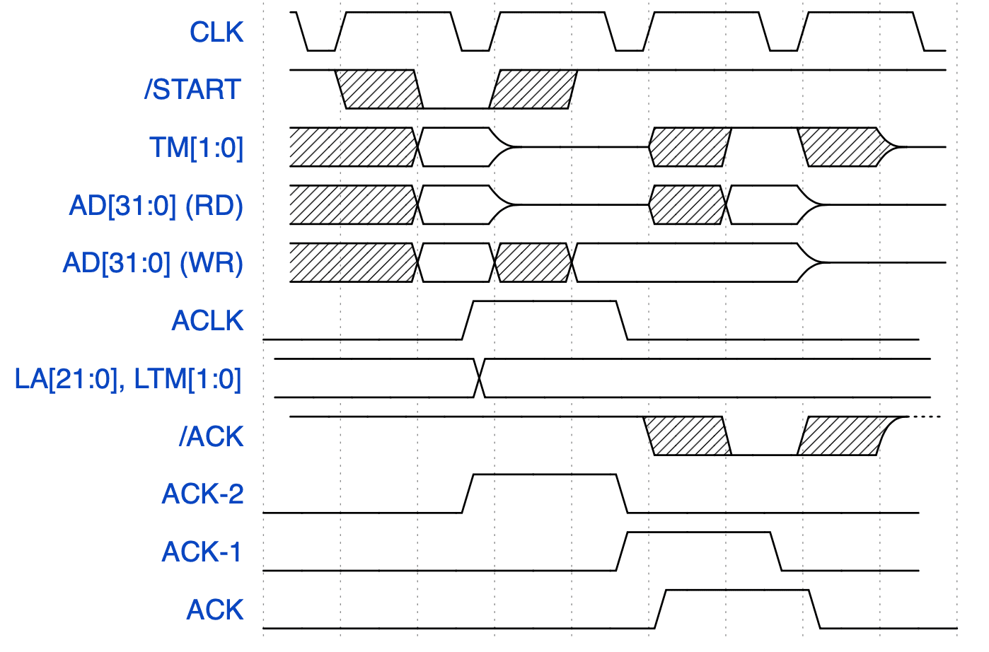
Screen Shot 2021-11-03 at 8.12.49 AM.png

Easy! ACLK is ACK-2. No gates required, just wires.


Moving on, we need to generate some /OE and /WE signals. Timing diagram:
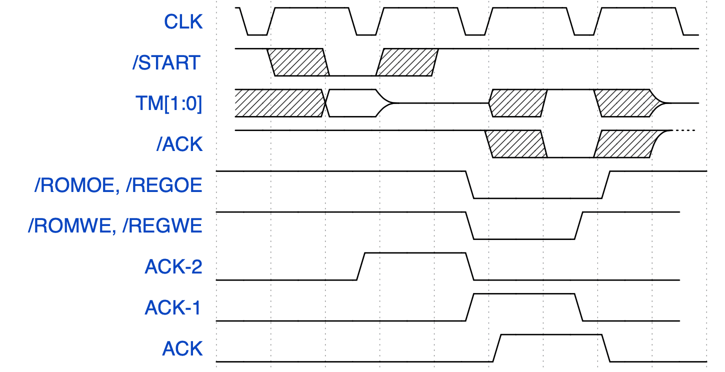
Screen Shot 2021-11-03 at 8.18.16 AM.png

/WE can fall whenever but should have a rising edge concurrent with CLK falling as that's when write data is considered valid on the NuBus. The /OE access time for 70ns flash ROM is like 35ns, then we need 21ns setup time for the data before the falling edge, and the data needs to remain valid on the bus until the rising edge of the clock. So /OE should rise right after the rising edge of CLK but having it fall a bit early (i.e. 3/4 through the single wait state in the middle of the bus cycle) is useful to add another 25 spare nanoseconds to our timing budget.

Here's the circuit for the /OE and /WE generation. LA[19] is the latched address bit 19 and LTM[1] is the latched TM[1] signal (indicates read/write). We basically just decode LA19 and LTM1 gated by ACK-1 or ACK-2 to get separate /OE and /WE signals for the shift registers and ROM. ROM is accessed when A19 is high (by declaration ROM convention) and the shift registers are accessed when A19 is low. ROM only occupies 8 bits of the 32 bit width of the NuBus so the status register (which has the PENDING bit) is read by the Mac in parallel with ROM. Similarly the control register (for twiddling the ESP32's reset pin) is written in parallel with ROM. So when you're writing ROM, make sure to put the right value in the ESP32 reset bit otherwise it'll toggle on/off, and when you're toggling the ESP32's reset, make sure not to invoke the coded command sequence used to flash the ROM.
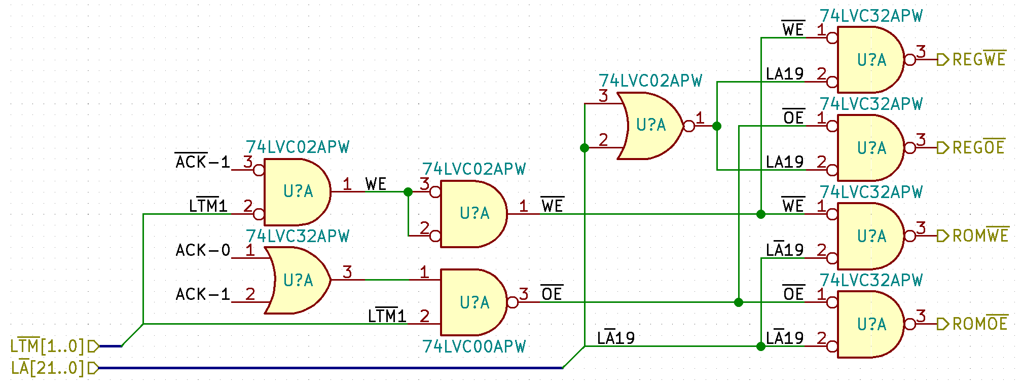
Screen Shot 2021-11-03 at 8.33.16 AM.png


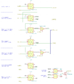
So now with the framework done we can implement the interesting stuff. Here we have the three control/status registers. On top is the ESP32 reset pin. You write to the ROM space and bit 0 (inverted) goes to the ESP32's reset pin. This register is reset by the system reset signal, unlike all the other registers in the system. Below are the pending bit registers. There are two. The first one just gets set when the shift register is written to. It's called /PENDINGE because it goes to the ESP32 to trigger an interrupt or whatever. The second register produces /PENDINGN (as in PENDING bit for NuBus) and is used for read back of the pending bit by the Mac. We have to register /PENDINGE to get /PENDINGN to ensure that it only changes after the rising edge of the NuBus clock.
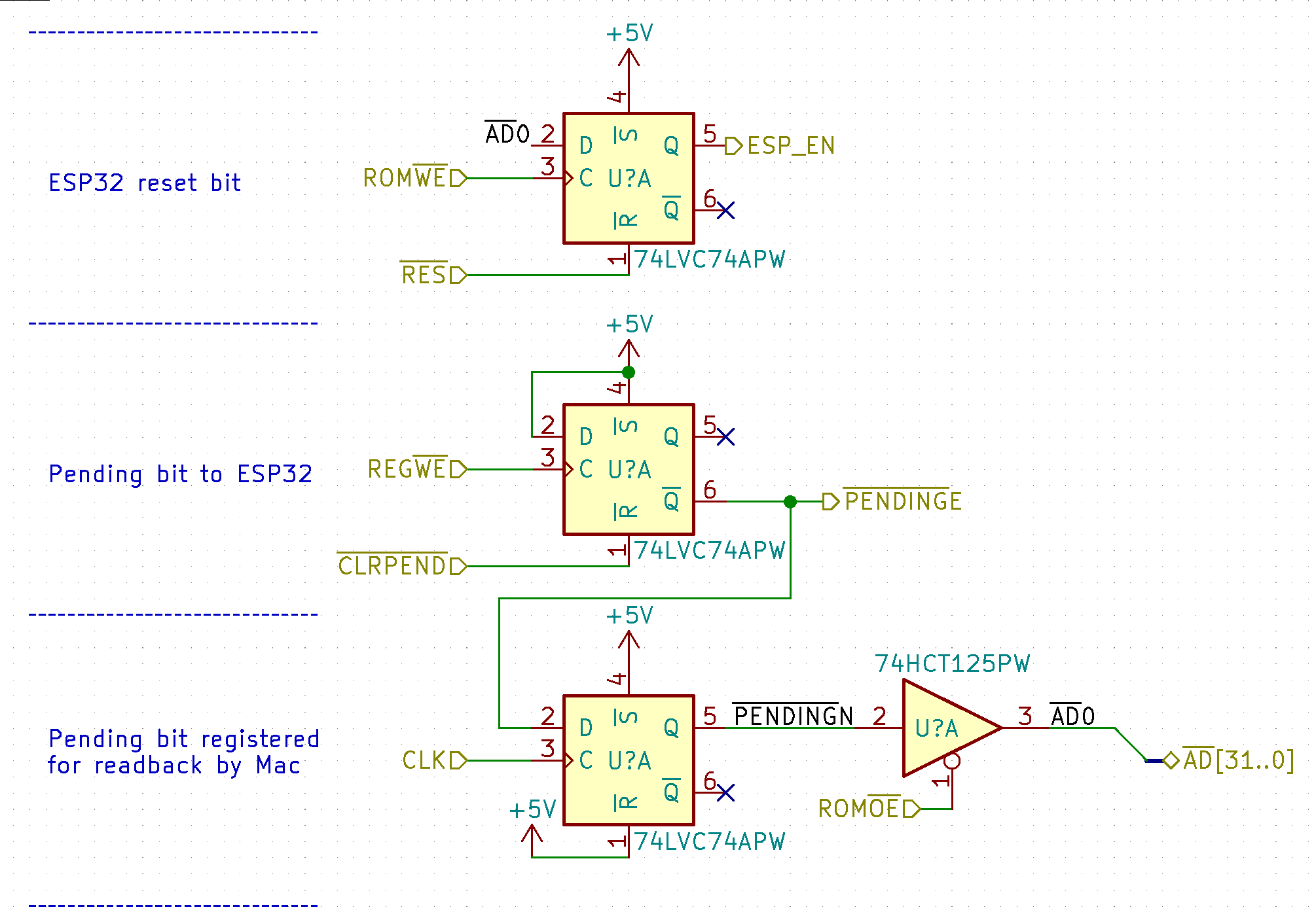
Screen Shot 2021-11-03 at 8.39.37 AM.png


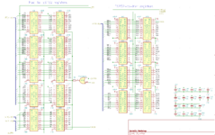
Now finally, the meat of it, the input and output shift registers. The left column is all the Mac-to-ESP32 shift registers. The /PL (parallel load) pin on the registers is hooked up to /REGWE, so when the Mac writes to the register space, the 32-bit data along with LA[5:0] get loaded into the shift register. The right column is the ESP32-to-Mac shift registers. The /OE on these is tied to /REGOE so they are output when the Mac reads from the register space. Also the output registers are cleared by /REGWE when the next command is written. All of the shift registers are connected to the SPI bus in series such that the Mac can pulse the SCK line 40 times to read the contents of the Mac-to-ESP32 off the MISO line while in parallel moving 32 bits of response data placed on the MISO line into the ESP32-to-Mac registers.
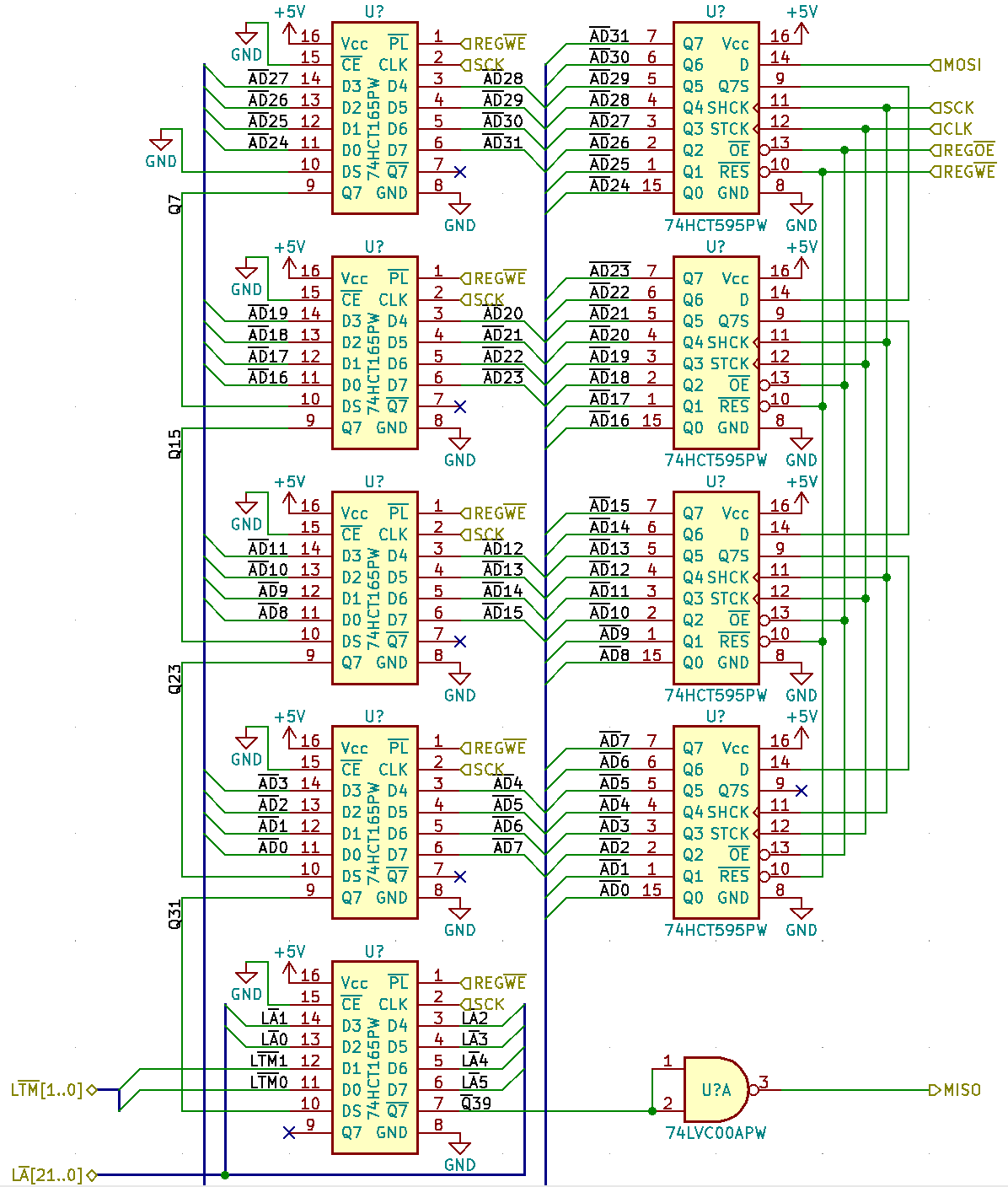
Screen Shot 2021-11-03 at 8.45.14 AM.png


Now for the loose ends, ROM and the aforementioned address register:
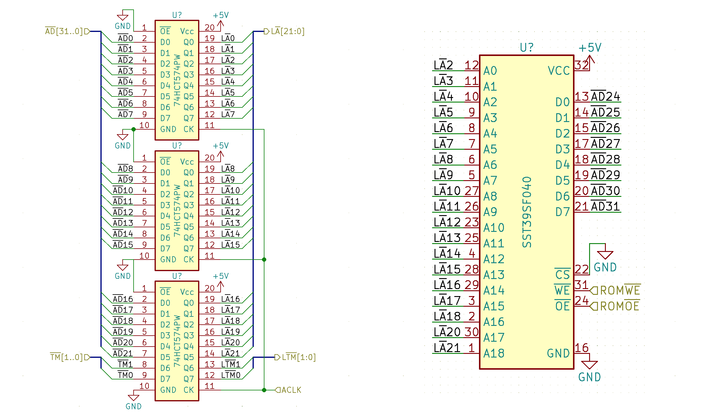
1635944716055.png


Does this make any sense? I’m just showing the NuBus interface because the ESP32 stuff is the same as on any ESP-WROOM-32 board. Total chip count is 25: 5 quad gates (74LVC: one of each '00, '02, '86 plus two '32s), 5+4 74HCT165/595 shift registers, 3 74LVC574 8-bit registers, 3 74LVC74 dual 1-bit registers, 1 74HCT125 quad tristate buffer, 1 39SF040 NOR flash ROM, 1 ESP-WROOM-32 module, 1 3.3V 1117-type linear regulator, and 1 CH340G USB-to-serial chip (for programming ESP32). Everything is new and you can have a board assembled with these components at JLCPCB but for the flash ROM and NuBus connector.

I hope this is at least somewhat clear! I stayed up all night doing this design lol so it's a bit hasty but I've had this idea for like a year and wanted to just get it out there.

I can implement the layout for this design but there's no software so it won't do anything. I know how to do a storage card but WiFi is more interesting and also harder. Storage can be an afterthought; I'd do the hardware for a storage card differently anyway. Can we discuss the various driver frameworks that we would have to work with to get Ethernet going? Is it easy to send raw ethernet packets with ESP32? I have only done high-level TCP/IP stuff with it. How do we add an ethernet interface to the Mac OS?
 
Last edited:

Zane Kaminski

Administrator
Staff member
Founder
Sep 5, 2021
372
610
93
Columbus, Ohio, USA
We can do that and it would be easier but it’s not as fun. The secret sauce is sort of in the Ethernet chip so if you use that it doesn’t feel as open-source, and it certainly wouldn’t as cheap to make.

My design has 25 chips but they’re all 7400 series aside from the ESP32 module, ROM, regulator, and CH340 USB-serial. The difficult part but also the strength of our project is that we have to define the command packet format to exchange data between the Mac and ESP32. Then we must write drivers for both the Mac and ESP32 that use the format we defined to do the requisite Ethernet stuff. So the software angle is hard but then we don’t need the sort of nuisance of a LAN chip which could be discontinued at any time. 7400 and ROMs are stable, and if Espressif goes belly up we can take our source and port to another WiFi chip. I wouldn’t wanna do the project if it was just gonna use an interface chip from someone else... not enough newness imo. I do the RAM modules with legacy chips but only because it’s basically impossible to do it differently.

In this case the extra work required to get it working on the ESP32 would be hard but would pay massive dividends. Lots of people are good at ESP32 programming. It would open up a whole world of possibilities... Bluetooth audio, keyboard/mouse, microSD storage, etc. All just limited by the programming skill of the contributors. As for the single chip advantage of a LAN chip, we could implement the logic I described in a CPLD but I’m trying to make it so you don’t have to agree to any EULAs or have a programmer or run a particular OS or whatever to make and develop for the card. Just click the button at JLC and then solder the connector and ROM socket on. ROM can be programmed by an app on the Mac.
 

Zane Kaminski

Administrator
Staff member
Founder
Sep 5, 2021
372
610
93
Columbus, Ohio, USA
Thanks to @alxlab I know what API I have to implement to do a Mac Ethernet driver. The API is so simple that the message format from the Ethernet driver on the Mac to the software on the ESP32 could just encapsulate the parameter block passed by the client of the Mac Ethernet driver to the ESP32. Responses from the ESP32 will require a bit more thought to the design but it should be easy enough.

Now the next real roadblock which needs solved before I continue much more is how best to convert 802.3 (Ethernet) frames into 802.11 (WiFi) frames and back. Obviously it’s possible (otherwise how would routers work) and I have seen multiple references from reputable sources (e.g. publications of the IEEE) that discuss the existence of a standard mapping between the two, but I can’t quite find a document laying it all out. Then I also don’t know how to get the ESP32 to send the raw 802.11 frames translated from 802.3, nor do I know how to hook in to get a call when a frame is received.

I have completed a draft schematic. (Attached) It omits the voltage regulator and some things are not connected to the ESP32 but it’s mostly complete and lays out the basic idea you get from following the "tutorial" in my first post.
 

Attachments

  • Schematic.pdf
    625.1 KB · Views: 115

Zane Kaminski

Administrator
Staff member
Founder
Sep 5, 2021
372
610
93
Columbus, Ohio, USA
Yeah, somehow the WiFi to Ethernet bridge has to get the packets received from the ethernet transciever and then retransmit them over WiFi. So it's basically the same software as we need for this but ours has to get the packets from the SPI interface connecting to the Mac instead of the ethernet chip.
 

alxlab

Active Tinkerer
Sep 23, 2021
287
312
63
www.alxlab.com
Yeah I hear ya. Was thinking maybe it would be possible to convert the packets of the Mac SPI interface into a normal ethernet signal and then pass that to the ethernet to wifi esp32 bridge. I guess that's really hacky though.

I did find this though:

https://gitlab.freedesktop.org/lima...867bb22387db7c86b903291ad/net/wireless/util.c

These functions might give insight:
Code:
int ieee80211_data_to_8023_exthdr(struct sk_buff *skb, struct ethhdr *ehdr,
                  const u8 *addr, enum nl80211_iftype iftype)

int ieee80211_data_from_8023(struct sk_buff *skb, const u8 *addr,
                 enum nl80211_iftype iftype,
                 const u8 *bssid, bool qos)

And I found this really high level overview of of the conversion works in both directions which you've probably already seen:

https://titanwolf.org/Network/Articles/Article?AID=0396c1e1-9796-4257-94b9-b6b9e057002c
https://www.ieee802.org/11/Documents/DocumentArchives/1997_docs/71522.pdf
 
  • Like
Reactions: Zane Kaminski

Zane Kaminski

Administrator
Staff member
Founder
Sep 5, 2021
372
610
93
Columbus, Ohio, USA
These resources are great! It seems like there are enough examples that we should be able to achieve success, particularly the one from hackster.io which is basically exactly the same program as our desired application.

I'm doing the board now:
Screen Shot 2021-11-06 at 8.28.54 PM.png


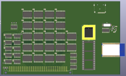
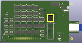
Everything from the schematic is on here plus dual footprints for the ROM... a PLCC-32 ROM/socket as well as a DIP-32 socket (as shown in the first picture). The DIP-32 and the NuBus connector are the only through-hole parts and obviously the DIP socket is not required if the PLCC ROM is mounted. Everything except for the microUSB I am using 1.27mm pitch or greater packages for so the board should be easy enough to assemble as far as surface-mount goes. The large size of even the smaller NuBus cards make it easy to fit all this stuff in such large (imo) packages.

Now the idea is to sort of stick the ESP32 out of the back of the Mac's case. Maybe we can stick it on a longer "peninsula" to get it even further away from the computer. I have to figure out how far backward something can stick out while not making it impossible to angle into one of the smaller Macs. Failing that there are ESP-WROOM-32 module variants with an IPEX (right?) jack for an external antenna.

One more thing. Interestingly, all of the components but the microSD slot are available in through-hole package... So I did consider a through-hole only board like so (using the ESP32-PICO-KIT V4.1 devboard):
Screen Shot 2021-11-06 at 3.32.31 PM.png

But I mean, someone else can do that if they want. You could even use a through-hole microSD breakout too, I just didn't wanna go that far down the through-hole road. So it's not my direction but I wanted to make sure the same hardware design could be redone with all through-hole components if desired, for a kit version for example.
 

alxlab

Active Tinkerer
Sep 23, 2021
287
312
63
www.alxlab.com
Regarding card dimensions:
View attachment 1636252784097.png
View attachment 1636252861270.png

There's more computer specific dimensions and clearances given in the Designing Cards and Drivers for the Macintosh Family by Apple Computer, Inc. I looked at the IIsi developer docs since I consider it a smaller Mac and it mentions "Any size NuBus card specified by Apple can be accommodated in the Macintosh IIsi computer." so should be fine with that computer.

Your card already looks like the short design so I don't think making the esp stick out would be that big of a deal especially if placing lower on the card.
Worse comes to worse can do something funky like add a db37 female connector to card and then put the esp32 on another card you connect with a male db37 connector:D

https://www.aliexpress.com/item/32972036701.html

Or yeah antenna... but that's not as fun.
 
Last edited:
  • Like
Reactions: Zane Kaminski

Zane Kaminski

Administrator
Staff member
Founder
Sep 5, 2021
372
610
93
Columbus, Ohio, USA
I have become aware of a new potential gotcha: SPI transfer overhead time on the ESP32. Reports online suggest that "polling" SPI transfers on the ESP32 can take up 5-10 microseconds after the relevant ESP-IDF API call to begin. This is way too much! On a 16 MHz ATMega328 the overhead is just a few clock cycles after writing to the right register. 10 microseconds to transfer 4 bytes would make for a speed of 400 kB/sec. Not awful but not great. So I have changed the design a bit and thought about some techniques to improve the per-transfer latency.

Hardware
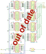
Unfortunately the 74...165 parallel-in/serial-out shift registers I was using to get data from the Mac to the ESP32 are only made in 74HC(T) and 74LV families today. These are alright but they're slooooow. 25 MHz max if you are designing to the worst-case specs. Also, JLCPCB wants you to do a minimum order of 1000 of the 74LVC595 shift registers I was using to transfer data from the ESP32 to the Mac. So I have redone the shift registers to use nothing but the more common 74LVC574 8-bit register. All of the shift/load functionality is accomplished through tristate logic. Downside is that there are 9 more chips... Check it out:
Screen Shot 2021-11-10 at 10.52.45 PM.png
This replaces this picture in my original post:
1636590197815.png

So that's nine more chips but there are some advantages. Firstly, we already had a '574 in the design and we have eliminated the five 74HCT165 and four 74LVC595 chips so although there are nine more chips, there's two less BOM lines. Secondly of course is the speed. I think this new 74LVC574 shift register setup will be able to do 80 MHz, the maximum speed for ESP32's SPI. This would reduce the data transfer time to get the 40 bits of data/address information out of the shift registers to 0.5 microseconds. So that knocks off a microsecond or so compared to running at 25 MHz.

I have also redesigned the status register slightly. Now there are two "pending bits" (as I called them before), one for sending data from the Mac to ESP32 and one for the opposite direction. Now they are called /RDREQ and /WRREQ. /RDREQ is low when the ESP32 wants to send data to the Mac and is cleared when the Mac reads that data. /WRREQ is low when Mac wants to send data to ESP32 and is cleared when ESP32 reads the data.

Another thing I have implemented is interrupt masking. The Mac should be able to receive an interrupt when any of the following occurs: new data from ESP32 to Mac, ESP32 finished reading data from Mac, or arbitrary interrupt from ESP32 (e.g. packet received). Therefore have added an interrupt mask register that can disable interrupt generation when new data is available from the ESP32 or when ESP32 has consumed data written by the Mac. General interrupts from the ESP32 can be disabled by sending the ESP32 a command.

Here's the new status register block with the bidirectional read/write requests and the interrupt masks:
Screen Shot 2021-11-10 at 7.21.25 PM.png

The new interface enables additional parallelism. Both the transmit and receive shift registers have two layers of registers. So when ESP32 intends to receive data from the Mac, it pulses the WRCLK. This clears the /WRREQ ("Mac requests to write data") signal and loads the data received from the Mac into the shift register where ESP32 can get it out via SPI. This way, the Mac can begin writing another 4-byte quantity into the register while ESP32 does the SPI transfer. Thus we only have to incur the worse of the two (ESP32, Mac) transfer times instead of the sum of both. It's similar for the ESP32-to-Mac shift registers on the right side but they have the shift+holding register arrangement internally so we don't need two sets of them.

Software
Moving on to the software, there are several sources of overhead in ESP-IDF when starting an SPI transfer. We should rewrite the polling portion of the SPI driver to remove these sources of overhead.

Firstly, there are a bunch of parameter checks in the ESP-IDF function that starts an SPI transfer, called spi_device_polling_start(...). We can just take that stuff out and make sure not to pass invalid parameters to our SPI transfer function. The SPI driver is thread-safe so a lock is taken out on the particular SPI peripheral used. We can just remove the locking stuff and only use the SPI port connected to the NuBus interface from one thread. Then the SPI driver calls setup_priv_desc(...) which allocates buffers if a DMA transfer has been requested and creates a spi_trans_priv_t SPI transaction parameter struct from the spi_transaction_t that was originally passed to spi_device_polling_start(...). Then (somewhat bewilderingly) spi_new_trans(...) is called which ignores most of the spi_trans_priv_t stuff that was just created and uses the original spi_transaction_t to build a spi_hal_config_t which is passed to spi_new_trans(...) and actually used to load the SPI device registers... All of these structs and functions have some purpose but only for modes which we do not intend to use. This setup process must be contributing to the 5 or 10 microsecond overhead that people are referring to.

So we can copy the contents of spi_new_trans(...) into our own SPI transaction start function, remove the extra stuff, and call that directly rather than going through the other few functions with all their parameter checking and optionally setting up buffers and whatnot.

I also thought I'd say something about the polling method of data transfer. In order to transfer data, polling loops have to run concurrently on the Mac and the ESP32. My hope is that we can get the SPI overhead down to 4 microseconds/longword (still a very high imo) in order to achieve 1 MB/sec transfer rate. Obviously there is the possibility that during data transfer, the Mac or ESP32 might receive an interrupt and have to do a task switch. If the Mac gets an interrupt during data transfer, no big deal, since the ESP32 can just hang around busywaiting. Unlike the Mac, the ESP32 has a dual-core processor and isn't trying to run a responsive GUI, service the occasional serial byte sent/received, and transfer Ethernet data. But what if the ESP32 gets an interrupt in the middle of a data transfer with the Mac? Or what if when the Mac wants to send data to the ESP32, the ESP32 has just left the polling loop data transfer task?

The Ethernet driver on the Mac should perform all data transfer at the "deferred task" level of the Mac OS. Deferred tasks are sort of like the Mac's version of reentrant interrupts. Deferred tasks are executed at the end of each interrupt service routine after all pending interrupts have been serviced and with interrupts enabled, so they can be interrupted themselves by another interrupt. This ensures that the mouse will stay responsive, serial data will continue to flow, etc. while data is transferred between the Mac and ESP32. (unlike during floppy accesses, for example, when the mouse gets all jumpy)

When an application requests to send an Ethernet frame, our driver will enqueue the first longword of data to be transferred to the ESP32 and the "write data accepted" interrupt will be enabled. Once ESP32 gets around to reading the data from the Mac, the write data has been considered accepted and the Mac gets an interrupt. During this interrupt, no data is actually transferred. Instead, the "write data accepted" interrupt is disabled and a deferred task routine is installed. It is in this deferred task in which the data transfer polling loop is executed and the remainder of the data is actually transferred to ESP32. If ever the polling loop exceeds some iteration threshold without any more data being transferred, that means that ESP32 has gone off and done a task switch. In this case, the deferred task routine reenables the "write data accepted" interrupt and returns. Once ESP32 gets back to the data transfer task, it reads the data previously posted by the Mac and then Mac gets another interrupt and sets up the deferred task again to transfer more data.

The algorithm is similar for reading data from the ESP32. The arrival of new data from the ESP32 causes a "read data available" interrupt, then the data transfer deferred task is installed and the interrupt disabled. During the deferred task, data is repeatedly transferred by polling loop until ESP32 stops answering, at which time the deferred task is exited and the "read data available" interrupt is enabled again.

Layout
The layout now looks like this:
Screen Shot 2021-11-10 at 10.52.12 PM.png

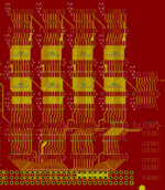
39 chips (!) but all of the logic chips are 74LVC, no more 74HCT. Fast! Cheap enough too and you can get it all at JLCPCB/LCSC except for the NuBus connector and ROM socket. The layout for the registers is very tidy:
Screen Shot 2021-11-10 at 10.59.14 PM.png

I'm excited! My next update will probably be a first attempt to define a command set that outlines what the Mac can ask the ESP32 to do.
 
Last edited:
  • Love
Reactions: alxlab and Stephen

Zane Kaminski

Administrator
Staff member
Founder
Sep 5, 2021
372
610
93
Columbus, Ohio, USA
Is it too crazy to put the WiFi module this far out the back of the Mac? Further from the case means better WiFi reception.
Screen Shot 2021-11-11 at 4.13.05 AM.png


1:1 scale (ish) comparison with real NuBus card:
IMG_4282.jpg


Maybe a little less? Right now it sticks out 1" from the board edge. Obviously the board edge is recessed somewhat from the end of the Mac's case so the actual protrusion beyond the rear of the Mac's case will be less than an inch, maybe half an inch. I guess it should stick out as far as a power cable. Is this any good?

I did another thing to help improve the speed performance of the big shift register chain that sends data from the Mac to the ESP32. The shift register has a gated clock (well, OR'd) in order to support serial shifting as well as loading of the shift register. Therefore the SCK clock incurs one extra gate delay (up to 4 ns) and this increases the overall clock-to-output delay of the shift register, eating up (in the worst case) all but 1.5 nanoseconds of setup time at the ESP32 at 80 MHz. Therefore I have added an additional pipeline stage with an ungated clock at the very end of the shift register. The ESP32's SPI hardware can be programmed to insert a "dummy bit" (i.e. an extra clock cycle) at the beginning of an SPI transfer. This increases the setup time at the ESP32 to 7.3 nanoseconds worst-case.

Here's the new bit of the data shift register schematic. U42B is the pesky but necessary clock gate that's increasing the delay in all the 74LVC574s, and U35B implements the extra pipeline stage with the ungated clock:
Screen Shot 2021-11-11 at 3.50.48 PM.png


Here are some notes aiming toward a spec for the NuBus interface and protocol between the Mac and ESP32.

Card Memory Map (1 MB slot space)
AddressSizeRead ActionWrite Action
$80000-$FFFFF524288 bytes (131,072 longwords)Read ROM (8 bits: AD[31:24])
Read RDREQ (AD[23])
Read WRREQ (AD[22])
Write ROM (8 bits: AD[31:24])
Write RDIE (AD[2])
Write WRIE (AD[1])
Write ESP_EN (AD[0])
$00040-$7FFFF524,224 bytes (131,056 longwords)Reserved (alias 00000-00003F)reserved (alias 00000-00003F)
$00010-$0003F48 bytes (12 longwords)Reserved (read data buffer)reserved (no operation)
$0000C-$0000F4 bytes (1 longword)Reserved (read data buffer)reserved (no operation)
$00008-$0000B4 bytes (1 longword)Read data bufferreserved (no operation)
$00004-$000074 bytes (1 longword)Reserved (read response data buffer)Write payload data buffer
$00000-$000034 bytes (1 longword)Reserved (read response data buffer)Submit command

Command Format
Commands are 32 bits long and can optionally be associated with a payload of up to 2048 bytes. The structure of a 32-bit command word is as follows:
(8 bits) command number
(24 bits) argument (referred to as Arg[23:0])

To submit a command to the ESP32, write the command word to the "Submit command" register in card space. To submit a command with a payload, write the payload into the "Write payload data buffer" register in card space, then submit the command word with payload data length parameter equal to the number of bytes written to the payload data buffer. The payload data associated with a command is always considered to be the most recent data written to the payload data buffer.

Command Set -- initial thoughts
Here are my thoughts on the bare minimum command set we need to support between the Mac and ESP32. All unused argument bits should be set to 0.
  • $0A -- Cancel Pending Command
  • $09 -- List Available APs
  • $08 -- Connect to AP
    • Arg[15:0] -- AP number to connect to
  • $07 -- Get Card MAC address
  • $06 -- Count Queued Transmit Frames
  • $05 -- Transmit Frame
    • Arg[10:0] -- frame length
  • $04 -- Count Queued Receive Frames
  • $03 -- Read Received Frame
  • $02 -- Enable/Disable Frame Received IRQ
    • Arg[0] -- enable IRQ if set
  • $01 -- Get Firmware Version
  • $00 -- Echo (NuBus interface loopback test)
    • Arg[10:0] -- echo data length
Command Response Format
The format of responses to a command should be standardized to simplify the implementation of the drivers. So a command response will be 32 bits plus a variable-length payload. The first 32-bit longword will have this format:
(8 bits) result code
(8 bits) return value
(16 bits) payload data length
 
Last edited:
  • Love
Reactions: alxlab

alxlab

Active Tinkerer
Sep 23, 2021
287
312
63
www.alxlab.com
How many pins of the esp32 module would you need to use? I'd still be tempted to design it with the module on a dongle or daughter board and use a connector like this:

1636664418397.png


Logic being that the card won't have anything sticking out besides connectors when installing into the computer. More importantly you'd be able to change the ESP module with different ones without having to modify the main board. You'd just have to make a new daughter board.

Downside is that it adds a few dollars to the cost of making the board.

Maybe it only makes sense on a dev board?
 

Zane Kaminski

Administrator
Staff member
Founder
Sep 5, 2021
372
610
93
Columbus, Ohio, USA
How many pins of the esp32 module would you need to use? I'd still be tempted to design it with the module on a dongle or daughter board and use a connector like this:

View attachment 933

Logic being that the card won't have anything sticking out besides connectors when installing into the computer. More importantly you'd be able to change the ESP module with different ones without having to modify the main board. You'd just have to make a new daughter board.

Downside is that it adds a few dollars to the cost of making the board.

Maybe it only makes sense on a dev board?
Oops sorry, I didn't directly respond to your point about the connector. The issue is sort of a long distance vs. short distance bus problem. Actually for 80 MHz operation, the ESP32 is as far away from the NuBus interface as it can be. Signals on a PCB propagate at about 0.16 nanoseconds per inch. The ESP32 is about 6 inches away from the shift registers, so that's 1 nanosecond of delay, and then another nanosecond of delay for the data out of the shift register to come back to the ESP32. 80 MHz corresponds to a 12.5 ns period, so 2 nanoseconds extra wiring delay for the clock to go to the 74xx chips and then the data out to come back is really significant. That's why I had to add the final pipeline stage at the end, to cut down on the clock-to-output delay as much as possible to make room for those two "wasted" nanoseconds going across the board.

It's really interesting how different buses solve this problem. As you approach 100 MHz, the physical size of the bus starts becoming significant even in a microcomputer system. The "radius" of a 100 MHz clock is like 5 feet. At these combinations of size and speed, you don't have system that can be considered to be all in the same clock cycle at the same time. A related topic is the DDR memory concept. Now DDR5 is going at 6.4 GHz. Multiple bits are in storage on the bus going to the RAM. The CPU is "ahead" of the RAM by several clock cycles, and it's sort of indeterminate how many clock periods of delay are consumed by the interconnect delay. Thus the RAM chips have to send a buffered version of the clock, called the data strobe, back to the CPU in order to properly frame the bitstream coming back on the data bus.

So long story short, I'm using SPI to connect the ESP32 to the NuBus interface. SPI is clocked and I wanna run at 80 MHz so in order to work over such a long cable, the NuBus slave would have to regenerate the clock (as I explained with DDR) and send it back to the ESP32 in order to frame the data on the MISO pin. You could do this but you'd have to use two separate SPI ports, one master and one slave, with the slave receiving the regenerated clock and the data coming back from the SPI device. Interesting idea (sort of copying DDR but much simpler) but the SPI slave max frequency is only like 10 MHz on the ESP32, so we could just clock the current setup down to 10 MHz from 80 MHz and then we could run the bus 8x further. But of course that's too slow.

UART, for example, is (by virtue of not actually being a "bus" by many definitions) immune to this kind of effect. You send some TX data. Receiver gets it eventually. It sends some RX data back. No need for anyone to be in the same clock cycle. Nobody takes turns communicating on the same wires and everything is assumed to be asynchronous. Same with PCIe, hence you can use those big long extenders and mount your GPU on the wall or whatever. The only penalty with the PCIE extender is latency and eventually the length degrades the signal too much and it stops working. But with DDR, it's a proper "bus" so the RAM chips have to regenerate the clock and send it back to the CPU and you can't use extenders.
 
  • Like
Reactions: alxlab

alxlab

Active Tinkerer
Sep 23, 2021
287
312
63
www.alxlab.com
Was thinking of plugging directly to the back of the card like:

1636668511807.png


But yeah. Just did a quick check of the physical size of the connector with relation to the card and don't think it would even fit with the USB, micro sd and HD44 connector side by side. With a normal Nubus bracket you only have around 74-75mm of board space. RIght now in that image it's taking like 80mm.

The connector itself would add roughly 25mm or 1" of length to lines going to the esp32.

Basing dimensions of the connect from

1636668915722.png
 

Zane Kaminski

Administrator
Staff member
Founder
Sep 5, 2021
372
610
93
Columbus, Ohio, USA
It would probably be better to move the JTAG, microSD, and USB interfaces onto the dongle board. Then all that needs to go through the connector back to the NuBus card would be power, SPI, and the few utility signals.

But is it worth it? It’d be stronger and the rear panel design would be more professional, as opposed to just a board sticking out the back. On the other hand, the dongle would take up a lot more room behind the computer than just the board sticking out, so it might not fit in all the places that people are currently putting their Macs. Also having the dongle would mean we would have to use a "real" metal rear connector bracket, though of course that would be more professional.

What’s the biggest benefit of the dongle design? Is it the sturdiness and professional appearance compared to the a peninsula of board sticking out the back?
 
Last edited:

alxlab

Active Tinkerer
Sep 23, 2021
287
312
63
www.alxlab.com
Also having the dongle would mean we would have to use a "real" metal rear connector bracket, though of course that would be more professional

I was assuming there would be a bracket regardless of whatever design is used. A metal bracket would be really awesome. I was thinking of designing a reference Nubus/PDS bracket for 3D printing which would be cheaper to make.

I'm not too familiar with the designing and cost of producing stamped metal stuff. Anyone here with experience in that area?

But is it worth it? It’d be stronger and the rear panel design would be more professional, as opposed to just a board sticking out the back. On the other hand, the dongle would take up a lot more room behind the computer than just the board sticking out, so it might not fit in all the places that people are currently putting their Macs.

I agree that having something stick out of the back of the wifi card can be a problem. If I wanted to go for a strictly professional appearance for a production wifi card I would probably focus on adding a antenna to the back of the card.

What’s the biggest benefit of the dongle design?

To me, the biggest advantage of the dongle / daughter board design would be mainly for development and testing purposes. I wouldn't use a connector, dongle or daughter board for the finished product.

On a dev board, the connector would let you test out different ESP32 modules / or maybe even other completely different modules with just replacing the dongle/daughter card and not the whole board.

A header or zif socket could probably be used to the same effect on the peninsula design, be cheaper, but would look less professional A header or zif could also be used on the card itself to attach a daughter board but then you would have to open the computer to swap.

Is it the sturdiness and professional appearance compared to the a peninsula of board sticking out the back?

I wouldn't consider it more sturdy since it's a removable part. Wonder what would happen if the ESP32 dongle was remove with power on? 😂

I guess what I'm basically suggesting in the end is the design a professional looking nubus to spi dev board instead of just a nubus -> spi-> esp32 board lol

From a design perspective this might not be possible. You've already mentioned the timing and such. Just getting exciting seeing the potential :)
 

Zane Kaminski

Administrator
Staff member
Founder
Sep 5, 2021
372
610
93
Columbus, Ohio, USA
@alxlab Hmm I have two ideas that should satisfy your desire for attaching SPI peripherals.

Keep in mind, the SPI-to-NuBus bridge is designed to connect to master devices on both sides. So the Mac addresses the bus bridge and then the bus bridge is accessed by the ESP32 to get the data out. So you can't really hook up an SPI slave peripheral such as an SD card, flash chip, accelerometer, etc. directly to the bus bridge.

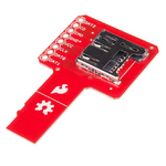
What you can do with the current design though is sort of piggyback off of the microSD slot. microSD cards are SPI slaves and there are microSD breakouts that you can buy, or make your own:
1636834625902.png
So you make your peripheral microSD-shaped on one end or connect your desired peripheral to an off-the-shelf breakout, then you reprogram the ESP32 to do whatever you want to the SPI slave in response to a command from the Mac.


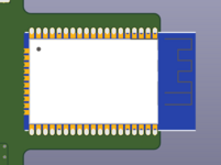
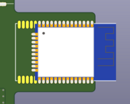
As for switching the WiFi module, I don't know if it would pay any great dividends to use something other than ESP32 now or in the near future. ESP32 is just so good! There is the new ESP32-S3 with Bluetooth 5 and more I/O but it also costs more. The good news about my design though is that the footprint can support both the ESP32-WROOM and the ESP32-WROVER modules:
Screen Shot 2021-11-13 at 3.20.54 PM.pngScreen Shot 2021-11-13 at 3.21.34 PM.png
The WROVER module is bigger and has 8 MB of RAM as well as 4-16 MB flash, as opposed to the WROOM which just has the flash and of course the ESP32's internal 576 kB SRAM. WROOM costs like $2-3 and WROVER like $3-4, whereas the new ESP32-S3 modules are $5+. There are also ESP8266-based modules but they are only slightly cheaper than the ESP32-WROOM modules and are significantly less powerful and flexible. Every vendor other than Espressif don't have the volume and ecosystem that the ESP32/ESP8266 have. So there's not much reason to switch to them at least for now.

It sounds like what you want is an FPGA-based development board! I was pondering an FPGA-based video card but I got stuck on the pin count. It requires quite a few pins to hook up to NuBus, SDRAM, and then have the 18-bit RGB parallel output to make the VGA signal. I wanted to use the Xilinx Spartan-6 FPGA on the card but the Spartan-6 in TQFP-144 package has basically exactly enough pins as would be required so no room for an SPI port explicitly. But what I can do is I can add a big header to tap the digital RGB signals on the way to the VGA DAC. That way you could disable the VGA DAC and then use the RGB/hsync/vsync bus as a 20-bit I/O port going to a daughtercard. I'll do it!

My new strategy is basically do to a bunch of "development boards" that are architecturally capable of some interesting function (WiFi, VGA, etc.) and then see if anyone wants to help with implementing the software and whatnot to make em work. I'm in the "NuBus state of mind" and I haven't quite fully absorbed the i.MXRT1170's documentation so the GHz ARM emulator board for the Mac SE will have to wait and I'll do the VGA NuBus card next. It's just one big FPGA and SDRAM plus the VGA so it should be easier to route than the big complicated hairball that is this board.

Edit: Picture of the latest layout:
Screen Shot 2021-11-13 at 8.57.57 PM.png
I'm gonna put some mounting holes for the card bracket on but I'm not following the usual NuBus placement conventions. The card will need a custom 3d-printed or stamped bracket. I'm gonna try and have the same dimensions on the VGA card too so the 3d models can be mostly similar except for the connector cutouts.

Honestly I'd like to put the microSD on a different edge than it's currently on. It's not meant to be hot-swappable and plugging one in with the power on will probably crash the ESP32 by browning out the 3.3V supply. So the microSD would be better on the top edge of the board to discourage hot swapping but I don't wanna endanger the microSD timings by putting it too far from the ESP32. I'll see if it can be done.
 
Last edited:
  • Love
Reactions: alxlab

alxlab

Active Tinkerer
Sep 23, 2021
287
312
63
www.alxlab.com
Sounds like a plan. I'll see what I can do to design a nubus face plate since I need one as well and it's something I can actually do :)
 

Zane Kaminski

Administrator
Staff member
Founder
Sep 5, 2021
372
610
93
Columbus, Ohio, USA
Here's the latest progress on the board:
Screen Shot 2021-11-17 at 8.26.39 PM.png


Almost done, basically I've just gotta pretty it up some more.

I've put the screw holes in the same places as on a NuBus card but the slots next to the holes have different dimensions to accommodate the larger width required for the 3d-printed material. So part of the bracket that attaches to the board can wrap around one side of the screw holes and attach to the plate portion of the bracket using two edges instead of one. Hope that makes sense; I'm not good at describing this kind of thing.
 
  • Like
Reactions: eric