Macintosh II Rev.A - Reversing the Discrete IC Implemented Origins of NuBus

Kai Robinson

TinkerDifferent Board President 2023
Staff member
Founder
Sep 2, 2021
1,023
1
1,059
113
41
Worthing, UK
OK well, from a quick glance so far - Apple P/N 343S1027 is identical in pinout and function to the Ti SN74BCT2420 - Nubus Bus Transceiver, available at UTSource: https://www.utsource.net/itm/p/1008026.html

The NuChip30, however? Made by Pinnacle Micro in Irvine, CA, by the looks of it. I lifted this from "Designing Cards and Drivers for the Macintosh Family" - page 86:

Screenshot 2022-06-25 011500.jpg
 
Last edited:

Trash80toG4

Tinkerer
Apr 1, 2022
772
236
43
Bermuda Triangle, NC USA
I think my notes are long gone, but ISTR deciding that the NuBus ChipSet in the DuoDock was a pure, Apple-unadulterated but rebadged TI product.

Which edition of DCaDftMF are you referencing?
 

Trash80toG4

Tinkerer
Apr 1, 2022
772
236
43
Bermuda Triangle, NC USA
Thanks, great resource. History of NuBus seems particularly relevant here as it was standardized in 1987, well after development of the Macintosh II, released March 2 that year.


LEM's article does a good job defining quirks specific to the Macintosh II.
 
Last edited:

Trash80toG4

Tinkerer
Apr 1, 2022
772
236
43
Bermuda Triangle, NC USA
OK well, from a quick glance so far - Apple P/N 343S1027 is identical in pinout and function to the Ti SN74BCT2420 - Nubus Bus Transceiver, available at UTSource: https://www.utsource.net/itm/p/1008026.html
Thanks, good to see the transceivers are available, once the Rev.A schematic is developed and compared to the IIcx schematic, four (possibly eight?) of the HAL ICs might be eliminated in order to implement the remainder on a test board?
 
Last edited:

Trash80toG4

Tinkerer
Apr 1, 2022
772
236
43
Bermuda Triangle, NC USA
The Radius IIsi NuBus Adapter and DuoDock II NuBus implementations would be what makes me think that a goodly portion of the Rev.A HALs might be excised from its NuBus chipset:

Radius_IIsi_Nubus.jpg


DuoDock_II-Block_Diagram.JPG


DuoDock_II-Functions_Diagram-NuBus.JPG


If NuBus MUX can be identified and eliminated from the Rev.A NuBus schematic, then the NuBus controller might be treated as a Black Box. If the three GALs on the Radisu IIsi NuBus Adapter can be read that would give us a leg up. They control but a single NuBus Slot keyed off the NuBus line present on the 030 PDS, but should give us a good handle on what's going down inside that Black Box in the Rev.A implementation I think?

@Bolle can those three Radius GALs be read?

DuoDock NuBus I've always figured was a standard TI Controller/MUX twins implementation. Thinking again would be that they're re-badged, stock parts from the TI Catalog?

DuoDock-Block_Diagram.JPG


Need to identify the four MUX/transceivers on the Dock II board, methinks they're standard parts that became available. In that case they'd be less expensive, have a smaller footprint and provide for much simplified routing as compared to the standard TI pair on the DuoDock board?

Docking Connector signals table . . .
 
Last edited:
  • Wow
Reactions: bakkus

Trash80toG4

Tinkerer
Apr 1, 2022
772
236
43
Bermuda Triangle, NC USA
From Duo System DevNote

Connections deleted for brevity: Address, Data, Power, GND, Docking Control lines, passthru connections for ADB, FDD, Serial, Modem, Sound, sleep etc.

Duo System Main Expansion Connector

Table 4-1 Main expansion connector signal assignments
Pin ___ Signal name ___ Description

9 ____ /STERM ______ Synchronous termination
10 ___ /DS __________ Data strobe
13 ___ /HALT ________ Halt
14 ___ /BERR _______ Bus error
15 ___ /BGACK ______ Bus grant acknowledge
16 ___ /IPL0 _________ Interrupt priority level signal 0 (least significant bit)
17 ___ /IPL1_________ Interrupt priority level signal 1
18 ___ /IPL2 _________ Interrupt priority level signal 2 (most significant bit)
40 ___ IOCLK _______ 15.6672 MHz I/O clock
41 ___ SIZ[1] ________ Transfer size bit 1

87 ___ /DSACK1 ______ Data size acknowledge bit 1
88 ___ /DSACK0 ______ Data size acknowledge bit 0
89 ___ /BR __________ Bus request
90 ___ /BG __________ Bus grant
92 ___ FC[1] _________ Function code bit 1
93 ___ FC[0] _________ Function code bit 0
94 ___ /RMC _________ Read-modify-write cycle
95 ___ CPUCLK ______ CPU bus clock
96 ___ /CPURESET ___ CPU reset (bus invalid)
116 __ RD __________ Read/Write
117 __ SIZ[0] ________ Transfer size bit 0
136 __ MI ___________ Memory controller inhibit for cache access
138 __ /SLOT E ______ IRQ Pseudo-NuBus expansion slot E interrupt
140 __ /IO RESET ____ Reset output to I/O systems

Interesting stuff, but not directly related to 030 PDS implementation of DuoDock

8 ___ /CIOUT _______ Cache inhibit out
85 __ /CBACK _______ Cache burst acknowledge
86 __ /CBREQ _______ Cache burst request

From this breakdown, it's clear that there are no dedicated NuBus Control lines, which leaves some possibilities

A ___ NuChip 34 represents a clean break from Apple's non-compliant NuBus implementation?
________ Slots are mapped from address and data lines, achieving CPU agnosticism of NuBus spec.
________ Makes sense, as from the beginning, Apple promised a PPC upgrade path for the Duo System
________ Apple later came to regret this and only grudgingly released the amazingly flexible 2300c board

B ___ NuChip_34 remains an Apple Kluge?
________ Slots are mapped to SuperSlot address space assigned to Slot E/$E interrupt
________ Slots are remapped to Address Spaces of Slots _ & _ as below

Occam's Razor would tend to support option A and Apple's use of an available, standard issue NuBus controller re-badged by supplier? But then again we're talking about Apple. :rolleyes: WAG would be that NuChip_34 was used in the Quadra series? First gen Q700 utilized some NuBus controller kluge labeled YANCC, again Apple. :rolleyes:

Haven't got DevNotes on hand for the rest of the Quadra series, my Technical Tomes are boxed up somewhere and the IIfx is buried under and behind more boxes. Really looking forward to getting things back together again after last of the slab's carpet is replaced.

The 40MHz bus implementation of the IIfx would be an anomaly. The one pic I have readily available has an Apple labeled ASIC with TI logo which appears to be its NuBus Controller? Anyone got spec on that handy?

Q840AV and its 40MHz bus would be another anomaly, what controller is used on that board?

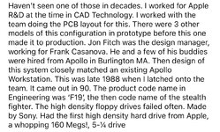
Duo System was developed for release in October of 1992, smack dead center of the morass that was Quadra development.

NuBus Controller
The NuChip 34 controls the interface with the optional NuBus cards. It is similar to the
NuChip 30, but with modifications that enable it to run at 33 MHz. NuBus cards occupy slot and super-slot segments C and D of the PowerBook Duo computer’s I/O space. (The flat panel video display occupies the address space normally occupied by NuBus slot 6. External expansion video and most I/O appear in the address space normally occupied by NuBus slot E.) Table 14-11 shows the I/O space for the NuBus cards.

Table 14-11 NuBus I/O space
Starting address __ Ending address __ Comments
F __ A00 0000 ____ FDFF FFFF ____ NuBus slot space
A __ 000 0000 ____ DFFF FFFF ____ Super slot space

______________________________________________________________________________________

Above was put together over coffee while in morning musing mode. Following up with a comparison of the slot address space defined above with standard NuBus Slot address space and related Block Diagrams will have to be done later.
 
Last edited:

Trash80toG4

Tinkerer
Apr 1, 2022
772
236
43
Bermuda Triangle, NC USA
Back to basics: the source of this stream of craziness would be the longstanding NuBus in SE/30 project. So I'm dialing the Rev.A reverse engineering back to the source of its 16MHz CPUCLK to 10MHz NuBus clock implementation for the moment.

If that's simple enough, such might be implemented on a rework of the Radius NuBus adapter for IIsi that "just works" just about fine at 8MHz in the SE/30? I've no need for the CoPro for an SE/30 version and doing a IIsi version with PDS passthru should work if using the SMT Ti SN74BCT2420 - Nubus Bus Transceivers @Kai Robinson found on either or both sides of a IIsi/SE/30 combo form factor hybrid?

I may be able to get that one figured out from Rev.A schematic development for comparison to the available Bomarc Rev.B schematic?

Dunno, coffee is catching up with my wetware so the images are going fuzzy, but I may be onto something?


edit: just thought of this, my brain doesn't grok conventional schematic, so can someone who's does read schematics identify the method for providing the NuBus clock from the NuChip Macintosh II schematic? That would save me diagramming the trace plumbing method I use to figure this kinda crap out. 😬
 
Last edited:

Trash80toG4

Tinkerer
Apr 1, 2022
772
236
43
Bermuda Triangle, NC USA
First step, go back to the source. First of series: DCaDftMIIaMSE

Figure_1-3_NuBus-RevA-DCaDFTMII-SE-04.JPG


We've got C16M (AKA CPUCLK?) and /CLK running in and out of this mess everywhere . . .

Now to compare this to the Bomarc NuChip schematic and maybe get this sucker up and running so I can measure the rate of /CLK? WAG is that it has to be 10MHz, nothing else makes much sense to this apprentice. Have we got a sorcerer online for comment here?

Never done this kinda thing, will one of my multimeters do or will I need to get some kind of USB doohicky, sillyscope kinda deal?
 
Last edited:

Trash80toG4

Tinkerer
Apr 1, 2022
772
236
43
Bermuda Triangle, NC USA
I love the images you chip de-constructors provide. How many layers does an ASIC like NuChip employ?

I'm wondering if my set of HALs might be shaved(?) and imaged for reverse engineering? Reproduction by burning GAL/PAL replacements would entail how much work? What might be the odds of successfully replacing them and booting up my Rev.A donor?
 

Trash80toG4

Tinkerer
Apr 1, 2022
772
236
43
Bermuda Triangle, NC USA
OK well, from a quick glance so far - Apple P/N 343S1027 is identical in pinout and function to the Ti SN74BCT2420 - Nubus Bus Transceiver, available at UTSource: https://www.utsource.net/itm/p/1008026.html
Morning musing of the day: This section of my Rev.A's HALs ought to be fairly easy to isolate from the State Machine HALs, no?

Thinking in terms of socketing that section of the board and doing a PCB that would be a plug in replacement for them? Conversion of their I/O to match that of the TI NuBus Bus Transceivers you found available might be wedged into such a plug in PCB?

Once that might be achieved, the State Machine HALs could be next on the list for socketing and experimental PAL substitution one IC at a time on another plug in PCB?

Suggestions PLEASE!

Looking for the best place to start on reverse engineering this mess after final carpet replacement is complete. Black boxing the HAL NuBus Bus Transceiver setup would appear to be non-trivial but achievable step given the comparison example of IIcx NuChip schematic?

@Melkhior what do you think of this approach to unraveling the mysteries of NuBus? We have several design examples of Bus Transceiver implementations in Apple machines and, especially so in the Discrete GAL state machines/stock transceiver IC implementation of the Radius IIsi NuBus adapter.
 

Melkhior

Tinkerer
Jan 9, 2022
98
49
18
@Trash80toG4 The SN74BCT2420 is a fairly simple chip, its only 'digital' job is to buffer (store) the sampled address and data information from/to the bus, under control of the SN74ACT2440 NuBus controller (if you use the full range of TI chips), and expose the buffered data to the controller. For NuBusFPGA, the sampling is done here, while the address is registered here or here, while the data is used directly from the sample (which unlike the address is valid throughout most of the cycle). The comparison is done here, my decoded_myslot signal is basically the same as the upper SN74BCT2420's /IDEQ signal (inverted).
Their 'analog' job is to push enough current on the bus when driving the signals, which a modern FPGA can't do (their drivers are likely too weak and can't handle 5V directly anyway); on the NuBusFPGA there's dedicated chips as drivers, 74LVT245 for A/D and 74LVT125 for other signals.

The state machines themselves are here (handling slave mode, so when some master such as the 680x0 is reading/writing to/from the device) and here (handling master mode, when the device is reading/writing to/from the host memory or another device [much less tested and debugged]). The trick is that those FSM currently talks to the internal Wishbone bus inside the FPGA. So when something on the Wishbone request to talk to some address mapped to that part of the Wishbone bus (i.e. the first 4 GiB of the address space, figure 1-9 in DCDMF3), a transaction is initiated on NuBus (test here).

To implement "host mode" (which is just a special kind of device where the memory is the slave function and the 680x0 the master function) one would need to replace this internal Wishbone bus by some mechanism that talks to the 680x0 bus (I believe the MAXI030 does that already for its glue) and initiate the transaction(s) in two FSMs. I'm not sure how Apple handled that exactly; aligned accesses are easy to understand, but I'm not sure what happens on non-aligned access from the 680x0 to NuBus (NuBus can't do unaligned, so the other way round is a non-issue). Presumably, one could use a logic analyzer connected to NuBus and PDS signals and see what happens when requesting unaligned data from a NuBus device.

The original Macintosh II implementation is still nonetheless interesting so see how it's done when using only minimal programmability (rather than a full-blow FPGA as I did, which is likely more resource-intensive), and also how the unaligned access are handled (... without breaking out the logic analyzer).

I think there's also the question of why do it at all (except as an intellectual exercise). If you want to re-use some specific vintage NuBus boards, there's still many usable NuBus-enabled Macs out there. If you want to interface a NuBus-less machine like the IIsi with some external 'standard' device (display, storage, network), might as well bypass NuBus entirely and design an extension board for whichever slot is available (PDS usually) - and that will be faster than forcing everything through NuBus. If you want to rebuild a new machine from a set of salvaged components, I could see the point, but again my suggestion would be to interface the devices directly with the CPU bus (PDS-like) for performance reasons.
 

Trash80toG4

Tinkerer
Apr 1, 2022
772
236
43
Bermuda Triangle, NC USA
I think there's also the question of why do it at all (except as an intellectual exercise).
That!

< TLDR >

However for me the exercise is more an exploration of the "artwork" that is a Logic Board's routing and "seeing" how all the components fit together within the copper Labyrinth. I can't "see" those connections on a conventional schematic, nor do I grok the code that you navigate so deftly.

For me, electronics would be a laboratory plumbing blueprint. I understand gates, valves, pressure regulators, backflow prevention, spillways and the function of their parallels in AND/OR/NOR logic (aced symbolic logic) resistance, diodes, zener diodes etc. but haven't had the chance nor interest in looking into anything more complex than Ohm's Law.

< wildly off topic background mode >

Pops was a mechanical engineer who, as the youngest guy on a team was tasked with learning how to put the new computer to work in auto parts design for production. After taking their test on a dare, IBM dragged him out of that world by the ears. There he became a Systems Engineer, manager in that field in a big branch office and finally one of the boffins at IBM's Glendale Labs.

Point of that tale would be that I "helped" my dad with his engineering homework by copying and drawing new diagrams while spending much time with him on the floor of the farmhouse as a pre-schooler. In grade school and high school I grew up with texts on machine coding, up through high level languages like COBOL and topping out with Pascal in the era of LSI and VLSI development. Those texts amazed me in terms of the artwork involved in the maze of electronics plumbing and engineering at the chip level. The layers of logic boards and ICs are graphic design elements translated into 3D chesslike wonders and sculptures with the addition of ICs, slots, I/O to the real world and such.

I fail to "see" the intricacies of the code in the links you've provided. Took an adult ed course in programming in Basic on Trash80s and wrote a loan amortization program while others struggled with the concepts of logic. Can code well I think, but don't particularly like it. Programming doesn't suit my stronger talents in art and craftsmanship so I haven't done it. I have boundless respect for it and those who've spent their lives mastering that craft (like my dad as a young man) while I've dabbled in PCB design, guiding the flow of electrons through the maze of components after having received praise that I'll take to my grave from true masters of other crafts.

< /wildly off topic background mode >

Again, I'm out of my depth in a project many would find pointless for very good reasons. But the journey is the point and so I've again tried to line up the pins as sorcerer's apprentice for masters of the craft to knock over one by one or many at once.

< /TLDR >

The aim of this exercise is but one part of a greater whole. That again is fitting NuBus implementation on a DIMM with control running up the one side and transceivers back down the other. That's one playground I've designed for experimenting with the blocks in diagrams of multiple machines using components of those Macs and off the shelf parts from TI and the like.

Grand scheme: teasing apart the IIcx board that @max1zzz has recreated to provide a playground for experimenting with many of your suggestions.

On the PSU end of a full size Macintosh II form factor board will be the three NuBus slots with the remainder of the system under the drive cages. On the way to the experimental NuBus DIMM Slot will be a pair of PDS Slots and a IIci Cache Slot for an Accelerator. Also curious to see if classic Cache boards can be teased into functioning in the IIcx and its kissing SE/30 cousin among other things

I see this as providing an erector set for those who might be interested in designing boards utilizing period correct methodology and components and a handy platform for those doing your thing. I love the work you and others are doing with modern tech, adaptation of FPGA to the world of classic tech.

I'm attempting a sponge dive into the classic boxes, retrieving the mooshy blocks from their diagrams and exposing the root structures of the critters beneath the surfaces of various Macintosh lids.

Coffee's kicking in, wondering if this stream of semi-consciousness makes any sense?
 
Last edited:
  • Like
Reactions: bakkus

jajan547

Active Tinkerer
Mar 25, 2022
732
295
63
North Carolina, USA
Thought you guys might find this interesting found this from a guy who worked on the team designing the iiFX for Apple apparently it's very similar to the Apollo Workstation.
 

Attachments

  • IMG_0856.jpg
    IMG_0856.jpg
    192.1 KB · Views: 38
  • IMG_0857.jpg
    IMG_0857.jpg
    433.2 KB · Views: 52

Kai Robinson

TinkerDifferent Board President 2023
Staff member
Founder
Sep 2, 2021
1,023
1
1,059
113
41
Worthing, UK
I'd love to be able to recreate the functionality of these chips in CPLD/FPGA form - so you could use them as replacements in Reloaded boards, or repairs.

I'm envisioning something like this: https://www.tindie.com/products/furrtek/neo-d0-replacement/ in terms of footprint, although you could use a thin flex-PCB header to link to an external PCB that has the logic on it, if it's not possible.

This image shows a castellated PCB with an FPGA on it as a chip replacement:

 
Last edited:
  • Like
Reactions: Androda

Trash80toG4

Tinkerer
Apr 1, 2022
772
236
43
Bermuda Triangle, NC USA
This image shows a castellated PCB with an FPGA on it as a chip replacement:

PCM-V1-.JPG


Wow, didn't realize folks were so actively pursuing this kind of thing? Thanks! I was thinking a castellated PCB was a higher/multi-level version of an interstitial adapter, but it refers to castellation of thruholes used to make contact?

I've been hoarding an advert for a patented industrial process: solder balling the bottom of an interstitial adapter for reliable QFP component replacement in production of existing designs. Been looking at that since dr. bob was trying to tell me that I couldn't get a G3 into my Duo 2300c twenty years ago on 'fritter.

Castellated VIAs of that pitch might work, how fine have you seen them done?
_______________________________________________________________

FWIW: Target for G3-on-603e development is low hanging fruit if anyone is interested. 😬
Develop that interstitial adapter to put ____forgot which G3?_____ on a Rev.1 PowerBook 1400c's cacheless 114MHz CPU board and bob's your uncle with the possibility of putting a G3 in 2300c or 5300 in his bag. 2400?

Reworking those CPU cards (more likely building them) might make a nice little service/product on its own. That's how Pismos got G4'd, no? Lots of 1400s out there. IIRC the Target CPU is faster and has more Cache on board than Sonnet's best has in DRAM on the extended processor board form factor in my 1400c.

Availability of the bottom surface of that card is what makes it low hanging fruit. A new PCB will need to be designed making use connectors that I believe are still available? Bottom surface of CPU card allows for placement of the crazy checkerboard quilt of passive components required on the underside of the PCB opposite the solderball connections of the CPU. So I probably still can't get the sucker in my 2300c, but one of you sorcerers might put that new build accelerator in this apprentice's 1400c?

I'm gonna just chuck this kinda craziness out there. I have too many ideas, too little know-how and way too little time left to do more than a very few of them. Any takers?
 
Last edited:

Trash80toG4

Tinkerer
Apr 1, 2022
772
236
43
Bermuda Triangle, NC USA
Back on topic of the history of Apple's NuBus implementations:

Found a Dock II board in the pile and have identified the quartet of Bus Transceivers from TI in the Block Diagram above:
74ACT16651 - 16-Bit Transceivers And Registers With 3-State Outputs - mouser.com 74ACT16651 at $14.64 ea.

So they're more expensive than the dedicated Ti SN74BCT2420 - used Nubus Bus Transceivers @Kai Robinson found, but they're brand new, straight thru, smaller footprint and simplify board layout significantly.

Moreover they're narrow, low profile SMT chips that'll make a nice little row between the soldertails of PDS passthru or PowerCache adapter connectors on a TwinFunction IIsi adapter or Multifunction/30 adapter which would be where all this tinkering with NuBus implementations would be ultimately headed. :p
 

Trash80toG4

Tinkerer
Apr 1, 2022
772
236
43
Bermuda Triangle, NC USA
Here's where things get interesting, Breaking the reverse engineering necessary to as few building blocks as necessary:

1) determine the NuBus Clock generation circuit in the Rev.A
2) isolate the HALs implementing its three state machine
3) Isolate the HALs implementing NuBus Transceiver requirements so they can be ignored.

DuoDock II NuBus setup is looking more and more intriguing in its apparent simplicity. All but the state machines and control present in its NuChip30/33 ASIC appear to be equivalent to HALs in Rev.A, which is dependent on the out of spec (all things considered, we can grant Apple some slack, we can say thery're PRE-Spec) NuBus ID lines.

Dunno about Macintosh II series in between, but the IIsi 030 PDSSlot NuBus adapter has a single NuBus ID/Control line present on the IIsi/SE/30 PDS pinout.

Here's where things get really interesting! DuoDock architecture appears to do away with NuBus ID lines? It supports of a pair of Slots! It is based on the pure as snow 030 PDS "Slot" that is the Docking Connector.

DuoDock II Takes us into the realm of off the shelf, available transceivers. Both Docks appear to use a 40MHz Clock in deriving 10MHz required for NuBus, making them CPUCLK independent? Very good news for the SE/30 and an overclocked IIsi board that!

DuoDockII-Block-Diagram-NuBus-Detail.JPG


DuoDockII-40MHz-Clock.JPG


Reference materials:

74ACT16651-pinout.JPG


74ACT16651-Pic2p.JPG


74ACT16651-logic.JPG