Project30_v6

Trash80toG4

Tinkerer
Apr 1, 2022
773
237
43
Bermuda Triangle, NC USA
Done playing with form factors, time to get on with the technical hurdles:

First approximation:
I was hoping that patching the three VIA2 signals to the three reserved pins on the SE/30 PDS would be sufficient.
Out of curiosity, are those pins grounded. Can't find my continuity tester ATM. :rolleyes:

No such luck:
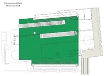
In the lower right corner of the IIcx NuBus Schematic Subsection there are two connections to UG11 on the IIcx which I haven't been able to locate on my @Bolle reworked SE/30 reloaded board. :(

Am I missing something?

P30-NuChip-pinout-dev-62.jpg.jpg


And WTHeck are those three red pins? ARST, HI0 , LO0 .PDF attached for markup.

Little help here gang? :oops:
 

Attachments

  • P30-NuChip-pinout-dev-62.pdf.pdf
    99.1 KB · Views: 66
Last edited:

Trash80toG4

Tinkerer
Apr 1, 2022
773
237
43
Bermuda Triangle, NC USA
A little last revision eye candy in the case that NUCHIP injection proves impossible:

Clean slate for the Radius IIsi NuBus Adapter rework approach:

P30-form-factor-062.jpg.jpg


Form factor is frozen and in the can! Here's proof of fitment and the card I'd be tempted to use if I had 040 Accelerator and GS Cards:

SE30-NuBus-Radius--Card.jpg


Four DSPs ought to give the 840AV a run for is money given enough Cache on the 040 Accelerator? Maybe?
With my P33 I'd be using the Futura SX/NIC combo.

@Bolle whatcha think? Is the reworked Radius adapter approach the way to go? Have you read out the GALs or looked at the schematic? From the looks of the NUCHIP CK input, methinks cutting the CPUCLK line and hanging a 40MHz crystal can off the requisite Radius Controller pin(s) might be sufficient?
 

Attachments

  • P30-form-factor-62-pdf.jpg
    P30-form-factor-62-pdf.jpg
    131.3 KB · Views: 34
Last edited:

Trash80toG4

Tinkerer
Apr 1, 2022
773
237
43
Bermuda Triangle, NC USA
@max1zzz thanks so much for the layers of your IIcx Redux.

I've reconstructed the traces/chips/pads for the three signals that meander down off NUCHIP in the NuBus section of the Bomarc Schematic.
Trying to figure out where ARST, LO0 and HI0 go and what they are doing?
Some of the circuit seems like it can be recreated on the NuBus Adapter side of the PDS?

Red = Solder Side Traces
Blue = Component Side Traces

Strange:
HI0 and LO0 are jumbled into multiple pins on one side or the other of resistors on the solder side?
ARST is connected to a pair of pins on a resistor pack?

WTF.jpg


How much deeper do you think I need to dive into this?
Next step would seem to be scouring the remainder of the pages for the ICs to see what might be up?