Se/30 c6 cap lead lifted
- Thread starter iantm
- Start date
You are using an out of date browser. It may not display this or other websites correctly.
You should upgrade or use an alternative browser.
You should upgrade or use an alternative browser.
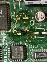
Seems the two pads are shorted together with solder, which needs to be rectified...

I can also see the tiny trace to which the pad sitting directly below the white + connects.
I've had one instance on an SE/30 board where I need to do a fix, but the trace leading to the pad was thicker. What I did was scrape off the green UV solder mask for 1cm of length on the trace leading to the pad. I then cleaned under the pad with 100% IP and used a microscope to flick away any debris, using an Razor blade knife. I left it 24 hours to ensure it was bone dry before doing the next step, which was to use a teensy tiny bit of 24-hour JB-Weld (the original stuff) to glue down the pad in its original location. Then I applied solder to the 1cm of trace length and reconnected the pad with solder. The cap I soldered onto that was short enough to where I could confirm the pad was still soldered to the trace.
But!
Your trace is super thin, so I cannot guarantee my technique would work.
@Branchus has a lot of experience rebuilding pads using very thin wire, and I think @Mac84 too, but I myself have never tried that, so maybe either of them could chime in with their recommendations.
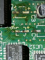
From what I could glean from 68kmla it’s “just” a mono sound connection. So if I can fix it by attaching the negative side of the cap to something on U11 (pin 7, apparently?) maybe it will work.My c6 cap on the se/30 board came dangling off - probably not enough heat or downward pressure.
what can I do about the lifted lead? Did I just brick my board?
Sorry, but which side is lifted? I had thought the + side was lifted and based my previous post on that assumption. You are speaking about the Negative side now, but is that side lifted? Or are both pads lifted? The photo doesn't make it clear. Because if it's only the NEGATIVE side lifted, you can follow my advice because that pad is thick enough, and you've got a thru-hole right there too.
I think it’s only the positive side? That’s how interpret the symbol on the board.Sorry, but which side is lifted? I had thought the + side was lifted and based my previous post on that assumption. You are speaking about the Negative side now, but is that side lifted? Or are both pads lifted? The photo doesn't make it clear. Because if it's only the NEGATIVE side lifted, you can follow my advice because that pad is thick enough, and you've got a thru-hole right there too.
My continuity meter registers something from the pad to the tiny trace.
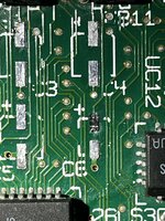
if it as all possible to tack that pad back down once I somehow free it from the glob of solder stuck to it, I can try.
I found this post about the same cap on 68kmla. At least I’m not the fist to sever the same lead.

SE/30 recap with lifted pad
Hi, My SE/30 started to show the "simasimac" lines last week. It displayed them for 6-8 minutes after which it gave the beep and started up normally. Reading about this told me that it was time for a re-cap. so i recapped my SE/30 today after receiving a recap-kit yesterday. It was somewhat...
Attachments
Last edited:
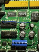
Thank you for the crystal clear photo of C6, showing solder removed and the Positive (+) side pad missing...

To follow MY advice, you would need to retain the removed pad, then try to clean out that black area under the pad with the tip of a razor blade like I did. The aim is to remove debris AND to provide a little depth below the pad where the JB weld will need to go to secure to the broken-off pad to the PCB. If you don't clear the blackened area as I just said, then if you apply a teensy tiny bit of JB Weld to glue-down the pad, that pad will sit raised up above the other pad. Maybe not a big deal, but it was to me, so that's how I did it.
But that super thin trace is the issue. Even if you clean off the green solder mask, there's not much trace-width for solder to stick. So you may need to run a thin galvanized (insulated) wire from that pad (after you glue it down) to wherever that super thin trace leads to. Then you are assured a good connection.
But again, Mac84 and Bruce may have their own way to replace the pad entirely using wire alone. I've seen Bruce do that in a video. I've never done it myself.
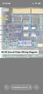
Makes sense to me. Dig a little trench for the pad then tack it down. Then either try and expose the trace or wire it to the U11. I’ve gathered the c6 is connected to the Sony sound chip. I found this diagram from recapamac points pretty clearly to the pin on the upper left (thank goodness for all this stuff being out there)Thank you for the crystal clear photo of C6, showing solder removed and the Positive (+) side pad missing...
View attachment 23865
To follow MY advice, you would need to retain the removed pad, then try to clean out that black area under the pad with the tip of a razor blade like I did. The aim is to remove debris AND to provide a little depth below the pad where the JB weld will need to go to secure to the broken-off pad to the PCB. If you don't clear the blackened area as I just said, then if you apply a teensy tiny bit of JB Weld to glue-down the pad, that pad will sit raised up above the other pad. Maybe not a big deal, but it was to me, so that's how I did it.
But that super thin trace is the issue. Even if you clean off the green solder mask, there's not much trace-width for solder to stick. So you may need to run a thin galvanized (insulated) wire from that pad (after you glue it down) to wherever that super thin trace leads to. Then you are assured a good connection.
But again, Mac84 and Bruce may have their own way to replace the pad entirely using wire alone. I've seen Bruce do that in a video. I've never done it myself.
Attachments
Sweet. Thanks for the confirmation… now this feels absolutely surmountable. Will be more careful with the second board though …
Buying a syringe of FLUX helps alot when soldering. It helps to ensure your joints are sound. Yes, it gets super messy with flux, and even though it can be left on the board, it's best to clean it off so it won't become a dust magnet, but it makes solder flow into tiny areas you never thought possible. It helps it from bridging adjacent pads by accident too, often times. There are different kinds of flux, but any kind is better than nothing, really.
I see your blue wire is one of those solid kind, possibly included with a breadboard kit. That will work, but if you accidentally hit it with your hand, or if something is placed atop your board, it will be strain on its two soldered joints. Probably not enough to break off the joint on the DIP IC, but maybe enough to break the teensy tiny join on the tiny SMD cap at C6.
If that blue wire wasn't shooting up in the air and instead was placed flat on the board, then you could put hot glue on it and it would never matter if it was touched. And while hot glue would work on your current wire suspended in air, you'd need more hot glue to truly secure it, and that would look a little tacky, perhaps.
Anyway, just a couple thoughts to share from my own experience, not criticism at all, mind you!
@JDW Absolutely no offense taken, I need all the help I can get!
I checked all my joints and reflowed a few of them that seemed weak or lifted off the pads. If I can get it working, I'll definitely tack down that wire. For now I"m letting it dry out after I gave it all a better cleaning with 99 IPA.
I've got a tantalum set of caps coming, I was going to try those on my second se/30 board (which does not have a ripped C6 pad). I'm aware that I have to flip my thinking because tantalums have the positive side marked.
If all else fails… I can send them to Amiga of Rochester.
Then I'll try and figure out why I'm not getting any sound. My SE FDHD and 800k are all fine in that regard. I have yet to actually hear the SE/30 chime!
In any case, I'm still having fun and I'm still hopeful!
Meaning, you submerge the entire board in 99% IPA? If so, that's what I do when I need to give the entire board a cleaning, usually to get rid of leaked capacitor fluid. I am filming a new video about recapping the LC520 motherboard, and I will dunk that one after my new capacitors are soldered in place....I"m letting it dry out after I gave it all a better cleaning with 99 IPA.
What I do is keep the board inside the IPA for no less than 30 minutes, then do a gentle toothbrush scrub, then leave it in a little longer, then scrub again in key places, then remove it, and drain it. I then put a floor fan on it for 24 hours. (99% IPA dries fast but when it gets under chips, it takes longer to dry.)
I've been a little afraid to dunk a whole logic board in, but I keep hearing that advice. I've got a big 'ole bottle of 99IPA. I'll grab a second and pour out enough to submerge the topside in a pyrex pan and do what you're suggesting. I hope I can get one of these working! There's always the SEs, but I'm optimistic I can get one SE/30 humming.
Last edited:
Some people who are much more adept at SMD work than I am go so far as remove entire SMD chips to clean leaked fluid beneath them, but I've not gone that far. Dunking the board is safer for me!I've been a little afraid to dunk a whole logic board in, but I keep hearing that advice. I've got a big 'ole bottle of 99IPA. I'll grab a second and pour out enough to submerge the topside in a pyrex pan and do what you're suggesting. I hope I can get one of these working!

But yes, pouring a lot of IPA atop the board is helpful too. Not quite as effective at breaking up gunk between tiny SMD chip pins as dunking, but with a fine toothbrush and the right scrubbing technique, pouring IPA can work.