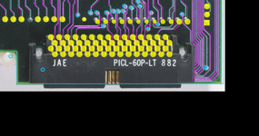
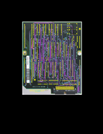
Second interaction with Mr. Claude Code, thought it might be interesting:
______________________________________________________
Maybe make a new discussion specifically addressing the reverse engineering of the PCB
Saved memory
Saved memory
Good to know — that changes how I should hand you stuff. Since you're working visually in Illustrator (even v8, which is EPS/vector-native and predates a lot of "modern" export assumptions), let's lean into that for the PCB reverse-engineering work rather than dense prose or spreadsheets.
Concretely, that could mean:
- Board maps as layered vector tracings — you photograph/scan the PCB top and bottom, place them as templates in Illustrator, and trace: traces on one layer, vias on another, component footprints on another, silkscreen reference on another. Classic RE workflow, and Illustrator handles it fine even at v8 (just watch out for spot-color / RGB vs CMYK defaults if this ever needs to go anywhere color-accurate).
- Functional block diagrams — instead of a schematic-capture tool, you draw the high-level blocks (VRAM, timing generator/PAL, bus interface, DAC/line driver) as boxes-and-arrows in Illustrator, which is often clearer for communicating "what talks to what" than a formal schematic anyway.
- Timing diagrams — HSYNC/VSYNC/blanking/porch waveforms as literal vector line art, which is actually a very natural fit for Illustrator and easier to annotate precisely than most scope software's export.
I can produce content for any of these as
SVG (which Illustrator 8 can import, though with some limitation since SVG postdates v8 — EPS is safer/native for that version) or plain
EPS, or I can just describe layouts precisely enough for you to trace by hand if you'd rather build it stroke-by-stroke yourself.
Given that, want me to:
- Draft the functional block diagram for the FPD card as a first visual piece (I can generate this as SVG/EPS now, even before you have the real board in hand — based on what's typical for this era/type of card), or
- Hold off on visuals until you've got board photos to work from, and instead keep building out the written RE spec section?
can you access this .PDF to see my progress? It's unlayered .PDF is there a way for me to upload an Illustrator 8 file?
Ran a command
Ran a command
I don't actually see a PDF in this conversation yet — the uploads folder is empty on my end. It looks like it didn't attach, so could you try uploading it again?
To answer your two questions directly:
Can I view a PDF? Yes — once it's actually attached, I can open it, view pages as images, and comment on your progress (layout, traces, whatever's in it).
Can you upload a native Illustrator 8 file (.AI)? This chat interface accepts uploads, but heads up on what I can actually
do with it:
- Old-format .ai files (v8 era) are essentially PostScript/EPS-flavored — I can inspect the file as text/binary and often extract path/structure info via script, but I can't open it in Illustrator itself or guarantee a clean re-render the way viewing a PDF or image does.
- If you export a PDF from Illustrator 8 (or even just save as PDF-compatible, which v8 supports as an option), that gives me the most reliable way to actually see it visually, layers or not.
- If it's genuinely unlayered already, that's fine — I can still look at it as a flat image/PDF, I just won't be able to toggle pieces on/off the way I could with a layered file.
So: go ahead and upload either the PDF or the .AI file (or both) and I'll take a look.
take a look at this:?
I don't see a file attached to this message — the upload didn't come through on my end. Could you try attaching it again? Once it lands, I'll take a look right away.
https://tinkerdifferent.com/attachments/fpd-schematic-010-pdf.30088/
Fetched:
https://tinkerdifferent.com/attachments/fpd-schematic-010-pdf.30088/
Fetched:
https://tinkerdifferent.com/attachments/fpd-schematic-010-pdf.30088/
That link resolved, but it came back as raw binary data rather than something I can render or read directly — my fetch tool can't parse PDF content from an arbitrary URL like that (I can only truly "see" a PDF if it's uploaded directly into this chat, where it gets processed properly).
A couple options:
- Download it and upload the file here — grab the PDF from that link yourself, then attach it directly to this chat. That'll let me actually view the pages/schematic.
- Tell me what's on it / describe key parts — if you just want to talk through what you're seeing (IC part numbers, crystal frequency, block layout), I can work from your description in the meantime.
Given this is presumably the
actual 1986 Radius FPD schematic someone's already reverse-engineered and posted (which would be a huge shortcut for your project — no need to trace the PCB from scratch if a schematic already exists), I'd really like to see it properly. Want to try uploading it directly?
How do I upload a file?
In this chat interface, there should be a
paperclip / "+" attachment icon near the message input box (usually bottom-left or left of the text field, depending on whether you're on desktop or mobile). Tapping/clicking that opens a file picker where you can select the PDF from wherever you saved it on your device, and it'll attach to your next message.
Quick steps:
- Download the PDF from that tinkerdifferent.com link to your device (if you haven't already)
- In this chat, click the attachment icon next to where you type
- Select the downloaded PDF file
- Send the message — I'll be able to open and view it once it's attached that way
If you're on the
mobile app, it's typically a "+" icon instead of a paperclip, same general location.
Once it's attached, go ahead and ask me to take a look and I'll dig into the schematic with you.
____________
PDF
Ran 4 commands, viewed a file
Ran 4 commands, viewed a file
I can see it now — and this is genuinely useful. A few things worth calling out:
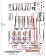
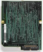
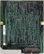
This is a solder-side PCB trace/placement drawing, not a logical schematic — and it's drawn natively in Illustrator (FPD-Schematic-010.AI8), traced from the physical board. Whoever made this did exactly the kind of vector board-tracing I mentioned earlier — good reference for your own workflow.
Let me pull a closer look at a couple of regions to read the labels more precisely before I summarize.
Ran 2 commands, viewed a file
Ran 2 commands, viewed a file
That's a great find — a few important details jump out:
Two selectable crystal oscillators, switched by jumper:
- JP1 → 55.000 MHz (marked TOYOCOM, part-ish "8853 JAPAN", "197.0556")
- JP2 → 51.270 MHz (marked "EC 1100", date code "89-09")
The silkscreen under the jumpers reads
"68K" / "64K" — worth flagging: that's likely OCR-me misreading (or the board's actual silkscreen) for what could be
"68Hz" / "64Hz", which would exactly match the naming in your spec (the 64/68Hz dual-mode board selecting between two pixel clocks for two vertical refresh rates via jumper). But it could also genuinely say "68K/64K" referring to a memory or configuration option unrelated to Hz. I'd treat this as
needs physical verification — worth checking the actual board silkscreen under magnification, since it changes how you read this circuit.
One more oddity worth noting: the 51.270MHz can's date code reads
"89-09" (i.e., ~1989), which is
later than your stated 1986 design date — meaning this particular populated board is likely a
later production revision or later-manufactured unit, not an original first-run 1986 board, even if the design itself dates to 1986. Worth keeping in mind if exact timing/component sourcing matters for your clone.
Let me look at the rest of the board — the DRAM/GAL logic block and the bus edge connector.
Ran a command, viewed a file
Ran a command, viewed a file
Good — this confirms and extends the picture. Here's a consolidated read of what your PDF actually documents:
What this drawing shows
A
solder-side PCB trace + placement map (per the title block: "Viewpoint = Solder Side, Light Blue Traces on Component Side") — i.e., you're looking at the bottom copper layer with the top layer's traces overlaid in a different color for reference. This is a two-layer board.
Component inventory (confirmed from the drawing)
| Ref | Part | Likely function |
|---|
| U13, U8, U17, U22 | GAL20V8-25LP | Programmable logic — sync/timing/address decode glue |
| U9 | GAL20V8-25LNC | Same family, different package/spec — another logic block |
| U18, U19 | ROM (unlabeled part #) | Likely boot/init code or a lookup table (possibly gamma/pattern ROM) |
| U16, U15(?), U12, U11(?) | µPD41264C-15 | 64K×4 DRAM, 150ns — this is your video framebuffer |
| U2 | SN74F109N | Dual JK flip-flop — likely divides/shapes a clock edge |
| U3, U4 | SN74F166N | 8-bit parallel-in/serial-out shift register — this is almost certainly your pixel serializer, shifting framebuffer words out to the video line at pixel-clock rate |
| U5 | SN74F161N | 4-bit binary counter — candidate for pixel/horizontal counter |
| U6, U7 | SN74LS393N | Dual 4-bit binary counter — candidates for horizontal/vertical timing counters |
| CR1–CR5, R1–R3 | Diodes/resistors near J1 | Likely output clamping/termination on the video line to the monitor cable |
Timing generation — this is the big one for your Section 1/2 work
You now have a real counter chain to reverse-engineer instead of guessing:
U6/U7 (393N counters) → U5 (161N counter) → U2 (109N flip-flop) → U3/U4 (166N shift registers) is a very plausible signal path from "raw oscillator" down to "serialized pixel data," with the GALs almost certainly generating HSYNC/VSYNC/blanking from taps off that same counter chain. Tracing the actual pin-to-pin connections (the colored traces) through this chain would let you derive H-total/V-total, and therefore blanking/porch,
without needing a scope — a nice independent cross-check against your planned analog capture.
Dual clock domain
Confirmed two crystal oscillators (55.000MHz / 51.270MHz) jumper-selected — strongly consistent with the "64/68Hz" dual-mode naming, pending verification of whether the silkscreen really says Hz or K.
Want me to redraw this as a
clean block/signal-flow diagram (SVG/EPS, so you can pull it into Illustrator alongside your own tracing) showing the U6→U7→U5→U2→U3/U4 timing chain hypothesis? That'd give you something concrete to verify pin-by-pin against the real trace colors.
WTF layer is unconfirmed first shot at buzzing connections. "Nancy's" would be traces I entered while visiting my girlfriend. I've done all work on project.
Good context to have — that explains both naming quirks:
- "Address & WTF?" = your first-pass continuity-testing guesses, unconfirmed, kept separate so they don't get mistaken for verified traces.
- "Nancy's" = just a session label (traces you added while visiting your girlfriend), not a second contributor or a separate methodology — so it's fully part of your own confirmed work, just named for when you did it rather than what it contains.
Good to know you've done all the work solo — that also means the ADDRESS/CONTROL promotion between -010 and -011 was you resolving your own WTF-layer guesses into confirmed traces, not someone else's contribution landing on top of yours. Makes sense.
I'll wait for the layer PDFs whenever you've got them ready.
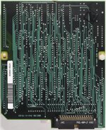
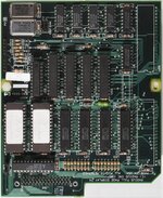
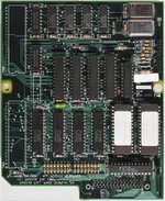
I will also upload high resolution photos of both sides of the board. Will also upload the "reversed" mirror imaged photo of the component side I use for reference. OCR of silk screen layer notations will likely be a good check against text input in what I call my "AI Coloring Books".
Recalled memory
This is turning into a substantial project — let me split it into its own area file so the details don't get lost, and keep your general working-style notes separate.
Created and edited memory
That's a smart cross-check — OCR'ing the silkscreen text gives you an independent verification pass against whatever you've manually typed into your traced layers, so any transcription slip (a "U13" mistyped as "U18," say) gets caught by comparing two independently-derived sources rather than trusting one read-through.
A few thoughts on what'll make this most useful once everything's uploaded:
- Board photos (both sides): I can inspect these directly and cross-reference IC part numbers, silkscreen text, and physical trace paths against what your traced layers show.
- Mirrored component-side photo: Good call keeping this — component-side photos need mirroring to compare directly against a solder-side trace view (since you're looking through the board from opposite sides), so having it pre-flipped means we're comparing like-to-like without me having to mentally flip coordinates.
- OCR cross-check: Once I have the photos, I can attempt my own read of the silkscreen text directly from the images and compare it against whatever text layer/labels you've entered in the AI8 file — that's a good three-way check (your typed labels, your traced positions, and an independent visual read).
I'll wait for the photos and layer PDFs — send them whenever they're ready, in whatever order is easiest for you.
Excellent, Reverse Engineering of the board is indeed its own project.
Makes sense — treating the PCB reverse engineering as its own project, separate from the signal-timing capture and scanline rotation transform work, keeps each piece scoped and easier to verify independently. The RE work you're doing now (layer PDFs, board photos, OCR cross-check) stands on its own as "figure out exactly what this board is and how it's wired," while the timing-capture and transform-spec work builds on top of that once the RE side is solid.
Happy to keep working with you on either thread as it comes in — just let me know which hat I should have on when you send the next batch of files.
How do I pull up either of the two projects for further work?
That depends on what you mean — here in this conversation, both threads (the RE work and the timing/transform work) are already live, so you can just say "back to the RE thread" or reference specific files and I'll pick up where we left off.
If you mean
starting a fresh conversation later and picking either project back up: I keep notes across our conversations, so you can just say something like "let's continue the Radius FPD clone" or "pick up the PCB reverse engineering" and I'll pull up what I have on file — the board specs, the layer names and what they mean, your naming conventions ("WTF?" layer, "Nancy's" layer, "AI Coloring Books"), and the general state of things. You won't need to re-explain the whole backstory each time.
One caveat worth knowing: I don't retain the actual files you've uploaded (the PDFs, EPS, AI8, photos) between conversations — only the facts and context I've written down. So if a new conversation needs to reference the actual schematic content again, you'll need to re-upload the file, but you won't need to re-explain what it is or why it matters.
That's great 1. open claude app 2. input text to pull up either project Upload all currently active files for each session as they're not stored on your end.
That's exactly right:
- Open the Claude app, start a new conversation
- Say something like "pick up the Radius FPD clone" or "continue the PCB reverse engineering project" — I'll pull up what I have on file (specs, layer naming conventions, project status) automatically
- Re-upload whatever files are relevant to that session (schematic PDFs, photos, layer exports) since those don't persist between conversations — only the notes about them do
That should get you back up to speed quickly each time without re-explaining the backstory. Good luck cleaning up those layers — looking forward to seeing the exports.