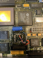
Floppy drive Sony MP-F51W-23 upper head doesn't touch the disk

billbucks

New Tinkerer
Oct 23, 2023
71
13
8
Thanks for your input. Attached is a photo of the UJ11 location where the blown chip has been removed. 3 of the connectors have been damaged (see photo) so I'm concerned I might not be able to solder a replacement chip should I find a dead Mac SE30 board ... Can it be fixed ?
Whilst I found the schematic of UJ11 here, I'm looking for a way to read the real chip pin allocation on the board i.e. where shall I start reading pin 1 and next ones? I noticed all chips are surrounded by 3 perpendicular corners and a single diagonal corner. I guess the diagonal suggests to start reading pin 1 from the top but I'm not sure. If this is correct, the broken connectors are 16,33,40. On the previous schematics, I can see that 40 is connected to A10, I don't see anything with 33, and I'm not sure if 16 is the one next to Part of UH7 that goes to the disc drive port.

If I can't find a replacement chip, would it make sense to connect some connectors e.g. via a 10kΩ resistor to +5V (ex : 20, 21 for the read/write select lines, and 38 for SEL SWIM ?
If I remove the ROM & RAMs, should a regular/working Mac SE 30 boot fine without the horizontal lines ? I'm getting lines with or with them.
 

Attachments

  • unnamed.jpg
    unnamed.jpg
    177.1 KB · Views: 64
Last edited:

billbucks

New Tinkerer
Oct 23, 2023
71
13
8
Someone suggested I could reuse the IWM chip from a Mac SE board (see photo) which I have.
Could it work ?

The corresponding pins could be determined from each board's schematics I guess.
 

Attachments

  • macseiwm.png
    macseiwm.png
    150.9 KB · Views: 45

JDW

Administrator
Staff member
Founder
Sep 2, 2021
1,884
1,598
113
54
Japan
youtube.com
You would need the newer SWIM chip, not IWM, because you are using an SE/30. @Kai Robinson created a PLCC-to-DIP adapter in the past, but it was never publicly released. However, you would need the opposite of that — a DIP-to-PLCC adapter. That would be rather awkward to solder on, even if it existed.

@Kay K.M.Mods has his own PLCC to DIP adapter here:

But again, you need the opposite of that, unfortunately.
 

billbucks

New Tinkerer
Oct 23, 2023
71
13
8
My intent is to remove the error screen and not use the floppy drive on the Mac SE30. If I use the IWM, could it solve this issue i.e. will the Mac SE30 be ok ?
I saw @Kay K.M.Mods project which is useful to identify the matching pins between both chips. Shouldn't it be feasible with a DIP28 and soldered wires to build a one-off custom solution ?
 

JDW

Administrator
Staff member
Founder
Sep 2, 2021
1,884
1,598
113
54
Japan
youtube.com
The difference between a "SWIM" and "IWM" is very important for the SE/30. As I said in my previous post, you need a SWIM, not an IWM chip.

So long as you have a SWIM chip and not an IWM chip, then it is merely a matter of figuring out how to wiring it properly to your motherboard, without making any pin wiring mistakes. But if connected properly, a DIP SWIM chip or a PLCC edition SWIM would work in your SE/30 motherboard.

But like I said, no one has a dummy-proof PCB solution for what you are seeking, which is to put a DIP SWIM onto PLCC SWIM pads (on an SE/30 motherboard).

And as I mentioned via PM, I am still waiting for a reply from the person I asked regarding your case. And I needed to ask because I have run out of ideas. You see, I've never had an issue with that chip, nor have a I tried to run an SE/30 board without the SWIM, so I cannot say what should happen when the chip is removed. I have been hoping someone else would jump into this thread and offer ideas, but thus far such has not happened.
 

billbucks

New Tinkerer
Oct 23, 2023
71
13
8
Thanks for your feedback.
The suggestion I got won't work so I'll look for a SWIM replacement unless I figure out how to wire some UJ11 pins to remove the error (these schematics can be useful). Attached is my understanding of the SWIM pinout ; is it correct ?
 

Attachments

  • swimpins.png
    swimpins.png
    181.5 KB · Views: 51

JDW

Administrator
Staff member
Founder
Sep 2, 2021
1,884
1,598
113
54
Japan
youtube.com
Incorrect.
Pin-1 is marked on the PCB and on the chip itself with a dot, and it should follow this diagram:

1742382577440.png


You also need to verify if the trace I've circled is broken, because it looks that way. It must not be broken.

1742381910490.png
 

Attachments

  • 1742382460288.png
    1742382460288.png
    26.8 KB · Views: 48
  • Like
Reactions: billbucks

billbucks

New Tinkerer
Oct 23, 2023
71
13
8
Hi,
I'm going to make an attempt to fix the board without floppy drive support.
Attached is an updated view of UJ11 connector's pins positions based on your reply.
I'm planning to connect pins 20, 21 and 38 to 5V, each via a 10K resistor. Does it make sense ?
Where should I find a suitable 5V output on the Mac SE30 board ?

I will also look at fixing the broken trace.

Thanks
 

Attachments

  • swimpins.png
    swimpins.png
    300 KB · Views: 15

JDW

Administrator
Staff member
Founder
Sep 2, 2021
1,884
1,598
113
54
Japan
youtube.com
Your pin numbering is correct for UJ11.

But you are saying that UJ11 pins 20, 21 and 38 need to be pulled-up to 5v via 10kΩ resistor. How did you determine that? Because on the schematic, I see pin 21 is tied to pin 24, and that is labeled READ DATA, shown to be an output according to the arrow direction...

1747992296100.png


Pin 20 appears to be Internal Drive Enable...

1747992354261.png


And I'm not seeing pin 38 on the BOMARC, but I did find it on the modern recreation of Apple's schematic, marked at HEDSEL...

1747992503298.png


The above schematic also shows VCC is +5v, but pins 11, 22, 30 & 44 are going to +5v through a ferrite bead (noise filter) at L21.


The BOMARC schematic is also saying this marking represents +5V...

1747991893601.png


So for example, the UE10 chip has pins 6, 26, and 35 all going to +5v...

1747991957245.png


You should reference the full schematic to see which pin of all the chips are going to +5v, and then you can pick which pin to tap.
 

billbucks

New Tinkerer
Oct 23, 2023
71
13
8
Thank you for your feedback. I indeed need to check that.
The initial fix was suggested by ChatGPT... (I don't always trust it but it can sometimes be relevant)
- It considered that Pins 20 (WR) and 21 (RD) and read and write signals
- It seuggested pulling D0-D7 data bus lines to +5 or GND
- It identified Pin 38 is as the address line to select the SWIM chip
- It suggested not to leave pin 43 (Apple Reset) floating i.e. +5V

Am I right to assume that pins 11, 20, 30 and 44 are connected to 5V (via the ferrite bead) so I could use either of them if needed.
I need to understand better how UJ11 works and what could be the expected values for the other Mac components to consider that the drive is disable and prevent any system error (currently the case with horizontal lines).
Unless the issue is related with something else.. I need to start with the broken wire.
 

JDW

Administrator
Staff member
Founder
Sep 2, 2021
1,884
1,598
113
54
Japan
youtube.com
Well, for important matters like this, I myself wouldn't trust ChatGPT, and I see you aren't either, which is good. We must also try to never "assume" either, which of course is why you are speaking to me in this thread. Well, the only thing I can do is what you can do — find pinouts and technical docs for the SWIM. I Googled and found this:


As you can see, it says pin 38 is HDSEL, and it describes it this way:
"This output may be used to select the disk side to read to or write from on some drives, or may be used as a general-purpose output (44-pin PLCC only)."

That same document shows the 44-pin PLCC pinouts too:
1748235267226.png


So that answers your question in the affirmative about whether pins 44, 11, 22, & 30 are Vcc. But you could possibly measure at those pins/pads with the machine on to confirm +5v is there.

The same document says pin 43 is overbar-DEV, which can be written /DEV or said "not DEV" and is described this way:
"This line is used to select the chip for reading or writing data from the processor."
The bar means it's Active LOW. So if tied to +5v, it would never be "active." The chip would never be selected for reading or writing data.

But please know that I am not an expert on the SWIM chips. I really don't know too much more about them than anyone else reading the aforementioned documentation.

You previously said your email is to get the board working without drive support. And it seems you want to try to disable the SWIM to achieve that. Now, that is yet another area which I cannot confidently comment because I don't know what the other chips on the board "expect." Even if you did all the right things electrically to "disable" or hide a SWIM or non-existent SWIM, would the other chips trigger an error that would lock up the board? That, I do not know.

But there are people out there more experienced than I am on the topic of the SWIM, so I will tag a couple

@Kai Robinson
@Bolle
 
  • Like
Reactions: billbucks

billbucks

New Tinkerer
Oct 23, 2023
71
13
8
Thank you for the link, it is very interesting.
I looked at pins linked with the CPU that would be worth connecting to the GND (pin 1) or 5V (pin 22 Vcc):
43 (/DEV = Device select) --> 5V
25 (/RESET) --> 5V
37/40/41/42 (A0-A3 : address lines) --> GND

Do I need to add a resistor before the 5V e.g. 10k ?
 
Last edited:

JDW

Administrator
Staff member
Founder
Sep 2, 2021
1,884
1,598
113
54
Japan
youtube.com
Again, I am no expert on these SWIM chips, nor do I have experience toying with them as you are. But any signal-level pins like RESET, DEV or even Address lines shouldn't be requiring a lot of current, so using pull-up or even pull-down resistors should be very safe and achieve your aims too. As to the resistor value required, it really depends on the current flow. But because we are talking about signal level pins here, I don't see why a resistance value of 10kΩ being chosen wouldn't work just fine.