There has been a recent commit for this project on github, and other commits in other projects. So probably just some delays and not enough time to post on TD.
WarpSE: 25 MHz 68HC000-based accelerator for Mac SE
- Thread starter Zane Kaminski
- Start date
You are using an out of date browser. It may not display this or other websites correctly.
You should upgrade or use an alternative browser.
You should upgrade or use an alternative browser.
Thanks!There has been a recent commit for this project on github, and other commits in other projects. So probably just some delays and not enough time to post on TD.
Bringup complete. 
Speedometer 3 results at 25 MHz are looking great:
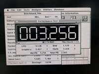
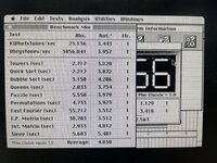
4.1x faster in "CPU" and 3.5x faster in graphics! I thought it would only be up to 3.8x faster. Huh.
Here's a video of the unaccelerated Mac SE doing the Speedometer 3 graphics benchmark:
And with the WarpSE:
Sorry for going incommunicado lol, I figured my limited time was better spent making Mac stuff than posting about unfinished products. Soon it will be beta testing time and then the release will be imminent after that!
Speedometer 3 results at 25 MHz are looking great:


4.1x faster in "CPU" and 3.5x faster in graphics! I thought it would only be up to 3.8x faster. Huh.
Here's a video of the unaccelerated Mac SE doing the Speedometer 3 graphics benchmark:
Sorry for going incommunicado lol, I figured my limited time was better spent making Mac stuff than posting about unfinished products. Soon it will be beta testing time and then the release will be imminent after that!
I don't know about everybody else, but I'm extremely excited by this update, Zane! Amazing work!
A little more on my development setup. I built this bus probe gizmo to let me directly connect the PDS bus to my logic analyzer. It has a female PDS slot on top so it can accept the WarpSE:
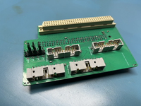
Along with a clip on top of the WarpSE's MC68HC000, this lets me probe basically all of the interesting signals in the system. Here's what it looks like on the lab bench:
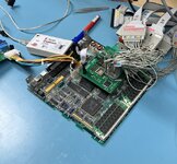
Kind of a big mess of wires but it gets the job done and lets me see everything going on on the analyzer. This is the kind of picture I get on the logic analyzer:
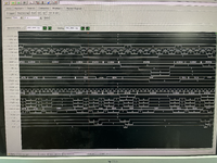
With the ability to look at both buses, I was able to proceed to debug all the problems and get the WarpSE working.
On another topic, the much-discussed sound issue is confirmed to occur right now on the WarpSE. I will have to stomp it out but it should be pretty easy. The solution is just to apply bandwidth rate-limiting on the sound RAM. It'll require some tuning but it should be easy enough now that everything else is working.
Edit: Also I figured I should discuss some changes to the WarpSE's final spec. The I/O bus bridge required quite a bit of frequency-specific latency tuning. Too little additive latency and the fast 68k might read data from the PDS bus before it's ready. Too much latency and the bus timing of two consecutive PDS reads will be slower than on an unaccelerated SE. This doesn't matter much because the WarpSE has onboard fast RAM and ROM, but nevertheless it would feel wrong to have some sequences of bus operations be slower on the WarpSE. So we're only gonna ship with a 25 MHz oscillator and omit the switchable frequency so we only have to do the tuning once for 25 MHz speed. MC68HC000 still has plenty of overclocking headroom at 25 MHz so nobody should be using 20 MHz. The motherboard ROM switch is also going away since it's not that useful of a feature. What I did add was the ability to disable the WarpSE by holding the programmers key while switching the Mac on

Along with a clip on top of the WarpSE's MC68HC000, this lets me probe basically all of the interesting signals in the system. Here's what it looks like on the lab bench:

Kind of a big mess of wires but it gets the job done and lets me see everything going on on the analyzer. This is the kind of picture I get on the logic analyzer:

With the ability to look at both buses, I was able to proceed to debug all the problems and get the WarpSE working.
On another topic, the much-discussed sound issue is confirmed to occur right now on the WarpSE. I will have to stomp it out but it should be pretty easy. The solution is just to apply bandwidth rate-limiting on the sound RAM. It'll require some tuning but it should be easy enough now that everything else is working.
Edit: Also I figured I should discuss some changes to the WarpSE's final spec. The I/O bus bridge required quite a bit of frequency-specific latency tuning. Too little additive latency and the fast 68k might read data from the PDS bus before it's ready. Too much latency and the bus timing of two consecutive PDS reads will be slower than on an unaccelerated SE. This doesn't matter much because the WarpSE has onboard fast RAM and ROM, but nevertheless it would feel wrong to have some sequences of bus operations be slower on the WarpSE. So we're only gonna ship with a 25 MHz oscillator and omit the switchable frequency so we only have to do the tuning once for 25 MHz speed. MC68HC000 still has plenty of overclocking headroom at 25 MHz so nobody should be using 20 MHz. The motherboard ROM switch is also going away since it's not that useful of a feature. What I did add was the ability to disable the WarpSE by holding the programmers key while switching the Mac on
Last edited:
...the much-discussed sound issue is confirmed to occur right now on the WarpSE. I will have to stomp it out but it should be pretty easy. The solution is just to apply bandwidth rate-limiting on the sound RAM. It'll require some tuning but it should be easy enough now that everything else is working.
... disable the WarpSE by holding the programmers key while switching the Mac on.
Much better than the Levco SuperMac SpeedCard I am using right now, which has the sound problem and doesn't have a fix, and which has a more bothersome method to disable the accelerator.
Absolutely fantastic, Zane!
Another interesting detail of the WarpSE is how it handles RAM refresh. As we all know, dynamic RAM must be refreshed and during the refresh, the CPU can't access the RAM, potentially slowing down the system. The WarpSE has an interesting way to mitigate performance loss due to refresh. The RAM on the WarpSE must be refreshed at least every 15.625 microseconds, so the WarpSE dutifully divides time up into 14 microsecond "refresh periods" and performs one refresh some time within each refresh period. That's the usual behavior for this kind of RAM system. The interesting thing is that each refresh period is further divided up. In the first 10 or so microseconds of the refresh period, the refresh request is said to be "non-urgent." In the final 4 or so microseconds, the refresh is considered "urgent" if it has not already been completed. Urgent refresh requests are completed as soon as possible and will delay a pending RAM access by the fast 68k. So therefore to minimize the impact of refresh, during the non-urgent window, the DRAM controller waits for a read from ROM or the slow PDS bus and then starts the RAM refresh. Since typical apps running on the WarpSE usually access a non-RAM device once every 14 microseconds, most or all of the time spent refreshing the RAM can be "hidden behind" periodic I/O and ROM operations. The net is a 1-2% performance gain. Of course when the RAM is not being refreshed (i.e. the other 99% of the time), the RAM runs with 0 wait states.
Last edited:
That's a beautiful design! I admire the RAM control logic - not that I understand all of it... Didn't know a CPLD could do that much, even a big one like this. But they're going to be expensive if Mouser is to be believed - you can get a decent Spartan 7 for that price! But the Spartan won't take 5V I/Os directly, of course :-( (and would need more extra support for config storage, etc., as well).
So exciting! Awesome, @Zane Kaminski! Thank you for doing all this.
I am really excited about this super cool project. I can hardly wait for it to be released!
There is also a bit more graphics performance to be squeezed out of the WarpSE. Due to a logic mistake, writes to video memory were taking five clock cycles instead of four. Fixing this amounts to a 1% speedup in graphically heavy workloads.
Fortunately we own a hundred or so XC95144XLs so we don’t have to buy any more to do the first production run. The WarpSE was kind of designed from stock. We already owned a lot of the CPLD, RAM, and flash and so I needed to make something to use up the rest of those parts.
Yeah, I think one step at a time. Eventually we will redo the WarpSE and eliminate all legacy parts including the 68k, asynchronous DRAM, and parallel flash. The DRAM and flash can be replaced by a single SDRAM chip plus a little serial NOR flash to store the ROM image. And of course we will need a big FPGA to replace the 68k. That’s in the future though.That's a beautiful design! I admire the RAM control logic - not that I understand all of it... Didn't know a CPLD could do that much, even a big one like this. But they're going to be expensive if Mouser is to be believed - you can get a decent Spartan 7 for that price! But the Spartan won't take 5V I/Os directly, of course :-( (and would need more extra support for config storage, etc., as well).
Fortunately we own a hundred or so XC95144XLs so we don’t have to buy any more to do the first production run. The WarpSE was kind of designed from stock. We already owned a lot of the CPLD, RAM, and flash and so I needed to make something to use up the rest of those parts.
Last edited:
My future to-do list has a few experiments:
Maybe I can also throw in some rudimentary mechanism for the PC to talk to the Mac as well. Right now when a PC is plugged in to the USB port on the WarpSE, the Mac is put into reset. So maybe I can change the way reset is handled and add a rudimentary interface to the PC in the CPLD. I have no idea what the interface would be used for. It's quite slow, like 300 bits per second if the bits keep alternating 0-1-0-1-0-1 but peaking at 500 kbit/sec when transferring a long string of 1's or 0's. So the connection is no good for networking or disk access. Sending data back to the PC is particularly slow. Even serial port is a bit of a stretch. It would be like "software serial" on an Arduino or something. Any ideas on what to use this for? I guess we could do keyboard and mouse since that's low data rate and basically all in the receive direction.
- Posted write buffer--how much does it improve performance? I have written a lot about the two word posted write buffer. This subsystem is part of the connection between the accelerated CPU and the PDS bus. The posted write buffer can store up to two video RAM writes so they complete immediately on the fast bus, allowing the fast CPU to continue executing from fast RAM or ROM while the updated video data trickles out over the slow PDS bus. But how much does this actually improve performance? I want to compare graphics benchmarks with both buffer entries enabled, just one buffer entry enabled, and posted writes totally disabled. This will inform whether future versions might benefit from deepening the buffer or whether its size can be reduced in future iterations to save cost and parts count.
- Overclocking--how fast can it go? Looks possible to achieve 30 MHz based on my logic analyzer traces. I've gotta dig out my big ol' Sony-Tektronix arbitrary waveform generator to output a variable speed clock and inch it up until the WarpSE stops working. The performance gains when overclocking also depend on the posted write buffer size so these two experiments should be done together.
- We're not using the DIP switches so let's get rid of 'em. Makes the board look cleaner. If we need to have any options they can be enabled by reflashing the firmware on the controller CPLD chip with a specialized version of the firmware.
- Somehow the data bit D0 of the fast bus got grounded everywhere in the prototype design. (!) We had to rewire it as a modwire on our prototypes. Interestingly enough, the first like 20 instructions in the Mac ROM are even-numbered (i.e. D0 is low) so it worked okay until the first instruction ending in a "1" lol. So I need to fix that.
- I was proud of only using a 25 MHz crystal (same as the 68k) instead of a 50 MHz crystal and dividing it by two, which is what all the Mac chipsets do. That was stupid of me lol. Most crystal oscillators don't have a controlled 50% duty cycle. The duty cycle could be 40%-60% or even worse. This means that the delay from the rising edge to the falling edge of the clock will not be the same as from the falling edge to the rising edge. The MC68k and CPLD do things on both clock edges so a duty cycle other than 50% means that the system is sort of running above 25 MHz for half of the clock cycle and the slightly slower than that for the other half. The uncontrolled duty cycle has been fine on the prototype but it worsens the timing margins, so we need to fix this. I'm gonna put a (slightly rarer and more expensive) 50 MHz crystal and then divide by two to get a 25 MHz clock with perfect 50% duty cycle. This duty cycle business is why the Mac chipsets have the 2x speed clock, not because of some inability to do it with the 1x clock... This will improve the timing margins when overclocking.
- No sockets! These surface-mount PLCC sockets are really unreliable. I have tried various vendors' sockets both cheap and expensive and there are a lot of problems. The larger sockets like for the PLCC-68 MC68k are prone to slowly ejecting the chip over time. I guess this is a well-known phenomenon and there is even an app note from Altera discussing it in the context of their CPLD chips. The small sockets like PLCC-32 frequently crack. I had a whole batch of 2 MB Mac II ROM SIMMs which had to be discarded for various reasons, including that some of the sockets were prone to breaking after a few insertion cycles. So unfortunately since we like selling really reliable stuff we can't include the sockets, especially not the for the 68k CPU. I'm planning on only using later mask revision MC86HC000s so there should be no speed issues and the CPU should never need to be swapped out. As for the ROMs, they can be reprogrammed in-system. You can probably even use the unmodified BMoW ROMinator program for this as long as it will run on an SE. This is a little bit risky because a power failure during ROM flashing will leave the ROM only half programmed, but a failure of that type is not unfixable by the end user. I can make a special firmware for the CPLD that boots from motherboard ROM and lets you reflash the fast ROM as long as you can get the ROM flash utility on the Mac.
Maybe I can also throw in some rudimentary mechanism for the PC to talk to the Mac as well. Right now when a PC is plugged in to the USB port on the WarpSE, the Mac is put into reset. So maybe I can change the way reset is handled and add a rudimentary interface to the PC in the CPLD. I have no idea what the interface would be used for. It's quite slow, like 300 bits per second if the bits keep alternating 0-1-0-1-0-1 but peaking at 500 kbit/sec when transferring a long string of 1's or 0's. So the connection is no good for networking or disk access. Sending data back to the PC is particularly slow. Even serial port is a bit of a stretch. It would be like "software serial" on an Arduino or something. Any ideas on what to use this for? I guess we could do keyboard and mouse since that's low data rate and basically all in the receive direction.
Last edited:
And of course we will need a big FPGA to replace the 68k.
I wonder if there is a further development of the FX68K FPGA or another FPGA that does the MC68k stuff?
I was really impressed with the Suska 68K10 core. There are a few other cores out there but they were all a bit obtuse and not so well tested. The Suska guy has been making 68k FPGA cores since 2000. He had an earlier core called the Suska 68K00 which started development in 2000 and was stable by 2012ish. Then he started the newer Suska 68K10 in 2014 (IIRC). Suska 68K10 had many releases over the next 7 years, and the 2021 release is said to be free of bugs and behaves identically to a hard MC68000 or '010. I instantiated it into a Lattice ECP5 FPGA a few months ago, but I couldn't get the timing simulation to go over something like 27 MHz. It could be that the timing analysis simulation was not properly constrained but just to be safe I'm not expecting a big performance increase if any when switching to the all FPGA approach.I wonder if there is a further development of the FX68K FPGA or another FPGA that does the MC68k stuff?
I was really impressed with the Suska 68K10 core. There are a few other cores out there but they were all a bit obtuse and not so well tested. The Suska guy has been making 68k FPGA cores since 2000. He had an earlier core called the Suska 68K00 which started development in 2000 and was stable by 2012ish. Then he started the newer Suska 68K10 in 2014 (IIRC). Suska 68K10 had many releases over the next 7 years, and the 2021 release is said to be free of bugs and behaves identically to a hard MC68000 or '010. I instantiated it into a Lattice ECP5 FPGA a few months ago, but I couldn't get the timing simulation to go over something like 27 MHz. It could be that the timing analysis simulation was not properly constrained but just to be safe
What about the Xilinx FPGA that is being used for the AppleSqueezer GS?
So far, it has been amazing for the Apple IIGS that blows out former accelerators and provides insane amounts of memory (which require an overhaul of the GSOS memory management to use that much memory). I wonder if Xilinx FPGA can be used to be a 68000 after putting the 68000 core in there?
Has anyone been able to extract cores from the 020, 030, 040, and 060? That is something to wonder about down the road.
I'm not expecting a big performance increase if any when switching to the all FPGA approach.
Oh, me neither. After all, it was not that needed back in the day. Just be nice if it sped up a bit, right?
It’s not so much extracting the core but rearchitecting it so it’s quite difficult compared to reading out a ROM. Anyway the AppleSqueezer uses the Spartan-6 which is a good FPGA and it used to be cheap but it has been in short supply lately and its future is uncertain. So I’m gonna use the Lattice ECP5 in the future although maybe I should investigate the Spartan-7 as Melkhior is always suggesting. Might be a little bit faster too and I get to use the Xilinx Vivado IDE which is apparently really good. I haven’t tried it.What about the Xilinx FPGA that is being used for the AppleSqueezer GS?
So far, it has been amazing for the Apple IIGS that blows out former accelerators and provides insane amounts of memory (which require an overhaul of the GSOS memory management to use that much memory). I wonder if Xilinx FPGA can be used to be a 68000 after putting the 68000 core in there?
Has anyone been able to extract cores from the 020, 030, 040, and 060? That is something to wonder about down the road.
Oh, me neither. After all, it was not that needed back in the day. Just be nice if it sped up a bit, right?
Indeed. As you mentioned the Suska cores look good, but unfortunately for later model not everything is open - the 68K30L is lacking the MMU, even though as I understand it internally a full version exists.It’s not so much extracting the core but rearchitecting it so it’s quite difficult compared to reading out a ROM.
Something I wondered about is the obsession for timing-accurate recreation in the Amiga world. Do they need it that badly? I'm fairly certain Macs don't. To create an accelerator, a '030-compatible design that's functionally correct is likely enough, instruction timings are unlikely to matter much. Only the bus needs timing accuracy, and that can be tested in a PDS device as when supporting bus mastering they basically reimplement the '030 bus.
Hehe, that' a case of 'if the only tool you have is a hammer...' As a newbie I started with Xilinx because they were market leader, so they were the one with the most examples and best third-party support in my perception. But there's benefits to using other devices, for instance the ECP5 you mentioned has decent open-source support (e.g. it can do this) in addition to the vendor's tool and can do very nice stuff (such as what this board supports).maybe I should investigate the Spartan-7 as Melkhior is always suggesting
