@JDW This business about the IWM and HD floppies is very interesting!! What exactly are the markings on your IWM? I do see a an interview with Steve Wozniak from 1984, before the SWIM but after the IWM, where he says the IWM can do "IBM format, double density recording":
https://downloads.reactivemicro.com/Users/Grant_Stockley/Apple2WozInterviewBYTE1984.pdf
Have we discovered this? Maybe it didn't quite work right and the PC/HD compatibility was not used until the SWIM? Or maybe James has a SWIM labeled as an IWM or something like that?
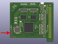
Anyway, I've got the new overclocking/debug connector on the side of the WarpSE:

There used to be some overclocking headers spread around the board but this new version consolidates everything.
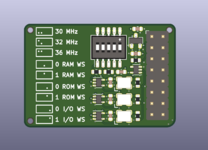
This little overclocking board goes in the overclocking connector:

You can select 30 MHz, 32 MHz, or 36 MHz, plus there are settings for RAM, ROM, and I/O wait states. My recommended settings:
| Speed | I/O Wait State | ROM Wait State | RAM Wait State |
| 30 MHz | On | Off | Try off, then on |
| 32 MHz | On | Off | Try off, then on |
| 36 MHz | On | Try off, then on | On |
I hear the Amiga folks run their 'MC68HC000s at 50 MHz so with 800nm parts these speeds oughta work fairly well but it's not guaranteed.
A little explanation on the overclocking options:
I/O wait state is recommended at all speeds 28.4 MHz or above. It doesn't really affect performance, but if not enabled the WarpSE's CPU could latch data from the PDS too early. So when overclocking above 28.4 MHz always turn it on.
On the other hand, adding a RAM or ROM wait state will decrease performance by about 20% but it might be necessary to achieve a particular speed. All WarpSE units are gonna have 60 ns DRAM and 70 ns flash ROM, but if we're lucky, the RAM could perform closer to 50 ns and the ROM closer to 55 ns (or even faster), since those are the next faster speed grades for the RAM and ROM respectively.
You have to know a bit about the WarpSE's timing budget to figure out how tight the timing is and whether you can get away without adding a RAM or ROM wait state.
For RAM accesses without a wait state, the WarpSE has basically 2.5 clock cycles to access it. The budget calculation is basically subtracting all the other delays in accessing the RAM from this 2.5 clock cycle amount of time. So to access the RAM, a series of things has to happen: the MC68k can take 20 nanoseconds to assert /AS, then the CPLD sees /AS and can take another 10 nanoseconds to assert the /RAS signal to the RAM, then the RAM takes up to 60 nanoseconds, then the MC68k requires the data to be ready 5 nanoseconds before the clock. You have to subtract these figures from the 2.5 clocks and the result oughta be positive to ensure it'll work. So for example, at 25 MHz, 2.5 clocks is 100 nanoseconds. Then you subtract those delays--20 ns, 10 ns, 60 ns, 5 ns--and there's 5 ns left in the budget. At 30 MHz, however, 2.5 clocks is only 83.3 nanoseconds. So if everything performs worst case, that blows the worst timing budget by 11.7 nanoseconds. So at 30 MHz, the RAM wait state may be necessary.
However, you could imagine that since we're using 800 nm MC68HC000s, and since the /AS signal is a really short wire just between the 68k and CPLD, that it won't take the whole worst-case 20 nanoseconds for the 68k to assert /AS. It might take only 16 ns for it to assert /AS. Then maybe we make up 1 ns in the CPLD (9 ns instead of 10), and maybe RAM is performing at 55 ns. And then the 800nm 68k probably doesn't need the whole 5 ns setup time so shave another 2 ns off... Well if everything is a bit faster like that, then we have spare time and conceivably 30 MHz will work without the RAM wait state. But maybe not if everything performs to worst-case specs.
However even if 30 MHz works without a RAM wait state, 32 MHz is less likely to work and 36 MHz even less so. So for 36 MHz in particular, the RAM wait state will almost certainly be required. With the wait state, then you get 3.5 clocks to access the RAM, which even at 36 MHz is plenty. However, adding the wait state reduces performance by 20% or so in RAM-bound workloads. So with the overclocking kit, you can experiment a bit and see what works for you.
ROM timing is better and also easier to calculate. For ROM, you get three clocks to access it, minus 20 ns for the 68k to put out the address, 70 ns to access the ROM, and then 5 ns data setup time at the 68k. So ROM definitely does not require a wait state at 30 MHz, and the worst-case ROM timing budget is only 1.25 nanoseconds short at 32 MHz and no wait state. So that oughta work if all we need is a spare nanosecond. However a wait state might be required at 36 MHz. Maybe not though since I think it's highly likely the 70 ns flash ROM will perform closer to 55 ns speed.
This oughta be good! Should boost the speed a fair amount. And of course I'm going to like 25.946 MHz on the production WarpSEs as well, since that squeezes all but the last nanosecond out of the worst-case timing budget. I think we may include this overclocking kit with the first bunch of units sold to get feedback and better understand the overclockability. Then later it might be an optional add-on. Not sure yet. Also if you're good at soldering it's easy to make your own little protoboard version with a through-hole oscillator and fixed soldered wait state options.


