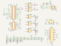
Too complicated! I think it's better to use the memory-mapped frame buffer approach than piping the commands over SCSI as the ScuzzyGraph does. And as for the MagicBus connector, I think we have to reject it in favor of the in-line expansion approach or nothing if there's not enough room. It's just not architecturally novel, which is what I'm usually going for. Maybe in a future version I can implement a buffered 3.3V fast bus slot. That would be more interesting!ScuzzyGraph and ScuzzyGraph II - Low End Mac
Online information about ScuzzyGraph is minimal. We do know that it allows old black-and-white Macs with SCSI ports to work with an external display. It supports a 3-bit, 8-color palette (some sources say 4-bit/16-color with some Macs), which is a far cry from the 8-bit/256-color output...lowendmac.com
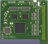
WarpSE basically has it!I would love a Brainstorm Accelerator for my Plus because of that bus accelerator.
Lemme say something generally about reverse engineering the BBU, BBA, etc. with the intent of cloning them. Why bother? Why not just make something new that conforms to the existing timings and functionality? Cloning the Brainstorm or BBU is okay, but the resulting product of the effort would be a subsystem that wants to be connected to a bunch of legacy chips in the particular arrangement of the Mac SE. And plus, getting it into the PLCC size and shape is not necessarily going to be cheap or easy. Why not just start with a blank canvas and make a new Mac chipset rather than a clone? I have some thoughts on this. If someone wants to do the board layout for a Mac SE reimplementation, I'll create the rough schematic and write the verilog for the FPGA.


